A method for starting a chip and a FLASH chip

A technology of chips and reference circuits, applied in information storage, static memory, instruments, etc., can solve the problems of long time and long time for FLASH chips, and achieve the effect of shortening start-up time, improving efficiency, and shortening the time of output voltage

Active Publication Date: 2018-12-14
HEFEI GEYI INTEGRATED CIRCUIT CO LTD +1
View PDF8 Cites 1 Cited by
  • Summary
  • Abstract
  • Description
  • Claims
  • Application Information

AI Technical Summary

Problems solved by technology

[0004] In the prior art, since the bandgap reference circuit is generally a closed-loop feedback loop, it needs to go through the process of positive feedback, negative feedback, and oscillation stabilization from start-up to stable output of the reference voltage. Therefore, the output of the reference voltage required by the bandgap reference circuit It takes a long time, which makes it take a long time for the entire FLASH chip to start and then return to the normal working state

Method used


Image

  • A method for starting a chip and a FLASH chip
  • A method for starting a chip and a FLASH chip
  • A method for starting a chip and a FLASH chip

Examples


Embodiment 1

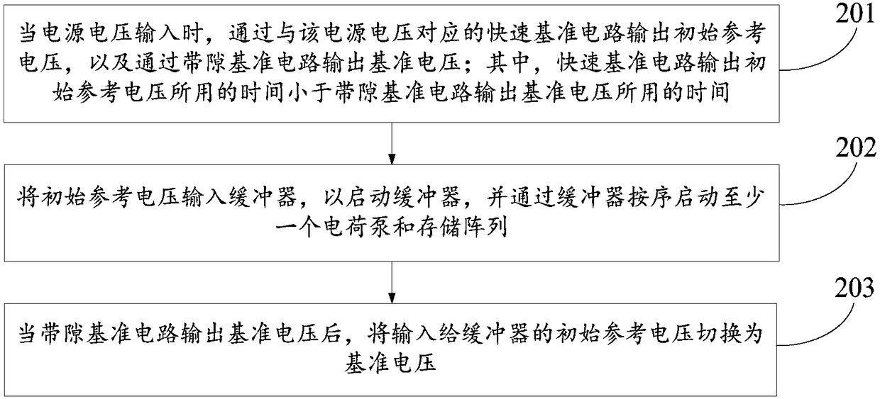
[0044] refer to figure 2 , shows a flow chart of the steps of an embodiment of a chip startup method of the present application, the method is applied to a FLASH chip including at least one fast reference circuit, a bandgap reference circuit, a buffer, at least one charge pump and a memory array, wherein , at least one fast reference circuit is connected in parallel with the bandgap reference circuit, and the parallel circuit composed of at least one fast reference circuit and the bandgap reference circuit is connected in series with the buffer, at least one charge pump and the memory array in sequence, and the method may specifically include the following steps :

[0045] Step 201: When the power supply voltage is input, output the initial reference voltage through the fast reference circuit corresponding to the power supply voltage, and output the reference voltage through the bandgap reference circuit; wherein, the time taken by the fast reference circuit to output the ini...

Embodiment 2

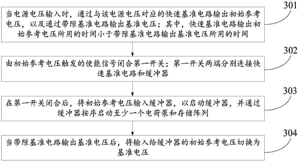
[0053] refer to Figure 3A , shows a flow chart of the steps of an embodiment of a chip startup method of the present application, the method is applied to a FLASH chip including at least one fast reference circuit, a bandgap reference circuit, a buffer, at least one charge pump and a memory array, wherein , at least one fast reference circuit is connected in parallel with the bandgap reference circuit, and the parallel circuit composed of at least one fast reference circuit and the bandgap reference circuit is connected in series with the buffer, at least one charge pump and the memory array in sequence, and the method may specifically include the following steps :

[0054] Step 301: When the power supply voltage is input, the initial reference voltage is output through the fast reference circuit corresponding to the power supply voltage, and the reference voltage is output through the bandgap reference circuit; wherein, the time taken by the fast reference circuit to output ...

Embodiment 3

[0083] refer to Figure 4 , shows a structural block diagram of a FLASH chip 400 of the present application, and the FLASH chip may specifically include: a fast reference circuit 401, a bandgap reference circuit 402, a buffer 403, at least one charge pump 404, a memory array 405 and a switch module 406; wherein, the fast reference circuit 401 is connected in parallel with the bandgap reference circuit 402, and the parallel circuit composed of the fast reference circuit 401 and the bandgap reference circuit 402 is connected in series with the buffer 403, at least one charge pump 404 and the memory array 405 in sequence.

[0084] A fast reference circuit 401, configured to output an initial reference voltage when the power supply voltage is input;

[0085] A bandgap reference circuit 402, configured to output a reference voltage when the power supply voltage is input;

[0086] Wherein, the time used by the fast reference circuit 401 to output the initial reference voltage is le...


PUM


Abstract

Embodiments of the present application provide a method for starting a chip and a FLASH chip. The method includes: when a power supply voltage is input, outputting an initial reference voltage througha fast reference circuit corresponding to the power supply voltage, and outputting a reference voltage through a bandgap reference circuit, wherein the time taken for the fast reference circuit to output the initial reference voltage is shorter than the time taken for the bandgap reference circuit to output the reference voltage; inputting an initial reference voltage into a buffer to start the buffer and sequentially starting at least one charge pump and a memory array through the buffer; when the bandgap reference circuit outputs the reference voltage, switching the initial reference voltage input to the buffer to the reference voltage. A fast reference circuit is added to the FLASH chip in the embodiment of the present application, and the initial reference voltage output from the circuit is used to start the buffer, the charge pump and the memory array, thereby starting the FLASH chip, greatly shortening the startup time of the chip and improving the efficiency of reading and writing data of the chip.

Description

technical field [0001] The present application relates to the field of chip technology, in particular to a method for starting a chip and a FLASH chip. Background technique [0002] FLASH is widely used in various electronic devices because of its advantage of keeping internal data from being lost even when the power is turned off. Usually, in order to save power, users can power off the FLASH when they do not need to use it. At this time, the FLASH enters a deep standby state. When the user needs to use the FLASH, the chip of the FLASH needs to be activated to restore the FLASH to normal operation. state. [0003] In order to facilitate the description of the process of FLASH recovering from the deep standby state to the normal working state under normal circumstances, the internal structure of the FLASH chip is firstly introduced. Such as figure 1 As shown, the FLASH chip mainly includes a bandgap reference circuit, a buffer, a charge pump and a memory array, and these ...

Claims


Application Information

Patent Timeline
Patent Type & Authority Applications(China)
IPC IPC(8): G11C5/14G11C16/30
CPCG11C5/147G11C5/148G11C16/30
Inventor 胡俊刘铭
Owner HEFEI GEYI INTEGRATED CIRCUIT CO LTD
Why Eureka
Try Eureka