A MOS transistor driving circuit for suppressing a driving voltage spike

A MOS tube, driving voltage technology, applied in circuits, transistors, electrical components, etc., can solve problems such as difficulty in choosing TVS tubes

Pending Publication Date: 2018-12-14
SHENZHEN YINGFEIYUAN TECH CO LTD
View PDF7 Cites 4 Cited by
  • Summary
  • Abstract
  • Description
  • Claims
  • Application Information

AI Technical Summary

Problems solved by technology

However, due to the limited maximum voltage allowed by the gate source of the MOS transistor, and in order to reduce the conduction loss, it is hoped that the driving voltage platform voltage of the MOS transistor should be as high as possible, resulting in a large difference between the driving voltage platform voltage and the maximum voltage allowed by the MOS transistor. Small, which makes it difficult to choose a TVS tube with a suitable voltage between the two voltage levels, and the existing drive circuit must be optimized

Method used


Image

  • A MOS transistor driving circuit for suppressing a driving voltage spike
  • A MOS transistor driving circuit for suppressing a driving voltage spike
  • A MOS transistor driving circuit for suppressing a driving voltage spike

Examples


Embodiment 1

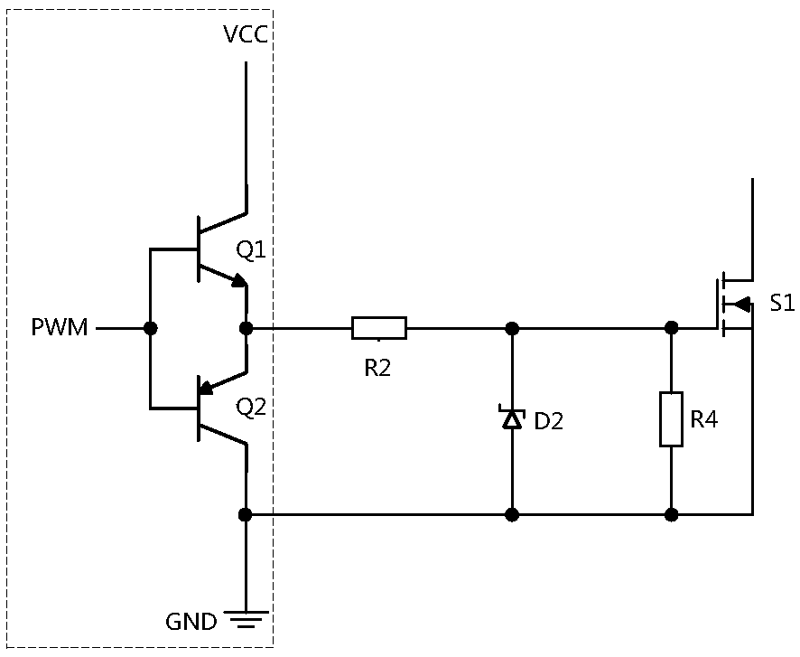
[0027] figure 2 A circuit diagram of the first embodiment of the power module burn-in system of the present invention is given. figure 2 In the above, the MOS tube drive circuit for suppressing the driving voltage spike and suppressing the driving voltage spike includes a push-pull circuit 1, a gate resistor R2 and an RCD absorbing circuit 2, and the push-pull circuit is composed of an NPN transistor Q1 and a PNP transistor Composed of Q2, the base of the NPN transistor Q1 and the base of the PNP transistor Q2 are connected to drive the PWM signal, the collector of the NPN transistor Q1 is connected to the power supply, and the collector of the PNP transistor Q2 The electrodes are connected to the ground level of the power supply, the emitter of the NPN transistor Q1 and the emitter of the PNP transistor Q2 are connected to the output end of the push-pull circuit, and the output end of the push-pull circuit is connected to the gate One end of the resistor, the other end of ...

Embodiment 2

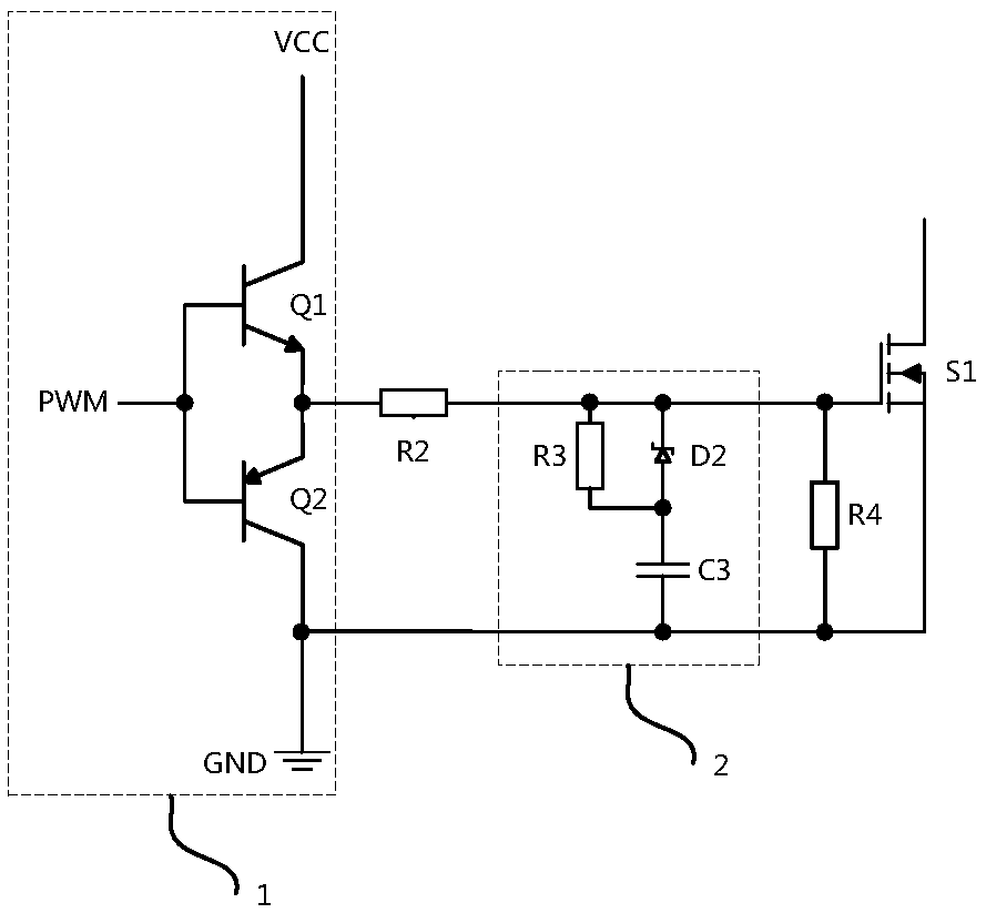
[0031] image 3 The circuit diagram of the second embodiment of the power module burn-in system of the present invention is given. image 3 In the above, the MOS tube drive circuit for suppressing the driving voltage spike and suppressing the driving voltage spike includes a push-pull circuit 1, a gate resistor R2 and an RCD absorbing circuit 2, and the push-pull circuit is composed of an NPN transistor Q1 and a PNP transistor Composed of Q2, the base of the NPN transistor Q1 and the base of the PNP transistor Q2 are connected to drive the PWM signal, the collector of the NPN transistor Q1 is connected to the power supply, and the collector of the PNP transistor Q2 The electrodes are connected to the ground level of the power supply, the emitter of the NPN transistor Q1 and the emitter of the PNP transistor Q2 are connected to the output end of the push-pull circuit, and the output end of the push-pull circuit is connected to the gate One end of the resistor, the other end of...

Embodiment 3

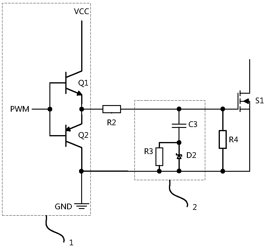
[0035] Figure 4 The circuit diagram of the third embodiment of the power module burn-in system of the present invention is given. Figure 4 In the above, the MOS tube drive circuit for suppressing the driving voltage spike and suppressing the driving voltage spike includes a push-pull circuit 1, a gate resistor R2 and an RCD absorbing circuit 2, and the push-pull circuit is composed of an NPN transistor Q1 and a PNP transistor Composed of Q2, the base of the NPN transistor Q1 and the base of the PNP transistor Q2 are connected to drive the PWM signal, the collector of the NPN transistor Q1 is connected to the power supply, and the collector of the PNP transistor Q2 The electrodes are connected to the ground level of the power supply, the emitter of the NPN transistor Q1 and the emitter of the PNP transistor Q2 are connected to the output end of the push-pull circuit, and the output end of the push-pull circuit is connected to the gate One end of the resistor, the other end o...


PUM


Abstract

The invention discloses a MOS transistor driving circuit for suppressing a driving voltage spike, includes push-pull circuit, an RCD absorbing circuit, a gate resistor and an MOS transistor, and is characterized in that: the RCD absorbing circuit comprises an absorbing resistor R, an absorbing resistor C and a TVS, the cathode of the TVS is connected with the grid of the MOS transistor, the anodeof the TVS is connected with one end of the absorption capacitor, the other end of the absorption capacitor is connected with the source of the MOS transistor, and the absorption resistor is connectedwith the TVS transistor in parallel. By adoption of the circuit provided by the invention, the gate-source positive driving spike voltage of the MOS transistor can be effectively suppressed by addingthe RCD circuit, and the turning-off reliability of the MOS transistor can be improved by adding a negative voltage circuit, and the MOS transistor driving circuit for suppressing the driving voltagespike has the advantages of simple structure, reliable performance and like.

Description

technical field [0001] The invention relates to the field of power electronic products, in particular to a MOS tube drive circuit for suppressing drive voltage spikes. Background technique [0002] In the existing power-type MOS transistor drive circuit that suppresses the driving voltage spike and suppresses the driving voltage spike, the push-pull circuit usually outputs a gate resistor connected in series to the gate of the MOS transistor, and a gate source is connected in parallel between the gate and the source of the MOS transistor. resistance. In practical applications, in order to prevent the interference coupling on the power line from generating peak voltage on the driving voltage, a TVS transient suppression diode is often connected in parallel between the gate and source to suppress the gate-source peak voltage when the MOS transistor is turned on. The circuit Such as figure 1 As shown, the reverse breakdown voltage of the generally selected TVS transistor is l...

Claims


Application Information

Patent Timeline
Patent Type & Authority Applications(China)
IPC IPC(8): H02M1/08H02M1/32H03K17/081
CPCH02M1/08H02M1/32H03K17/08104H02M1/0038
Inventor 柳树渡李茂华孙志新
Owner SHENZHEN YINGFEIYUAN TECH CO LTD
Why Eureka
Try Eureka