

Inorganic flexible transparent perovskite oxide voltage-controlled varactor and preparation method thereof
A technology of perovskite oxide and varactor, which is applied in the direction of variable voltage capacitors, etc., can solve the problem that flexible substrates are not resistant to high temperature, voltage-controlled varactors cannot be flexible and transparent at the same time, and substrates are not stable. With flexibility and other issues, it achieves the effects of excellent tuning rate, high light transmittance and wide application prospects
- Summary
- Abstract
- Description
- Claims
- Application Information
AI Technical Summary
Problems solved by technology
Method used
Image

Examples
Embodiment 1
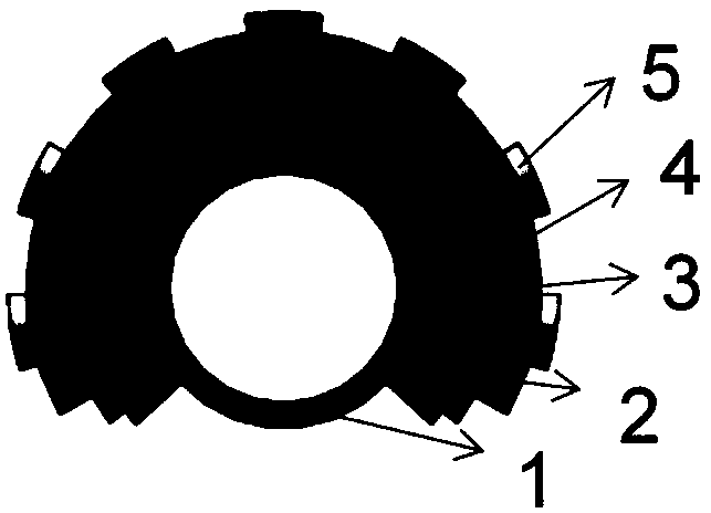
[0027] The specific preparation process of the inorganic flexible fully transparent perovskite oxide voltage-controlled varactor in this embodiment is as follows:
[0028] (1) Put the mica substrate with a thickness of 10 μm into the growth chamber of the sputtering deposition system and evacuate it, then raise the temperature to 300°C, and sputter-deposit Ag and ITO films in sequence. The thickness ratio of Ag:ITO is 1:10, and the layer The number is 2 layers, the total thickness is 150nm;
[0029] (2) (Ag / ITO) prepared in step (1) n The bottom electrode was heated to 650 °C, and Bi was deposited by sputtering 3.25 La 0.75 Ti 3 o 12 (BLT) thin film, thickness is 200nm, after treating that temperature is down to room temperature, take out the deposited BLT thin film;
[0030] (3) Cover the mask with the BLT film prepared in step (2), put it into the growth chamber of the sputtering deposition system and evacuate it, then raise the temperature to 300°C, sputter and deposit...
Embodiment 2
[0033] The specific preparation process of the inorganic flexible fully transparent perovskite oxide voltage-controlled varactor in this embodiment is as follows:
[0034] (1) Put the mica substrate with a thickness of 10 μm into the growth chamber of the sputtering deposition system and evacuate it, then raise the temperature to 300°C, and sputter-deposit Ag and ITO films in sequence. The thickness ratio of Ag:ITO is 1:10, and the layer The number is 2 layers, the total thickness is 250nm;
[0035] (2) (Ag / ITO) prepared in step (1) n The bottom electrode was heated to 650 °C, and Bi was deposited by sputtering 3.25 La 0.75 Ti 3 o 12 (BLT) thin film, thickness is 200nm, after treating that temperature is down to room temperature, take out the deposited BLT thin film;
[0036] (3) Cover the mask with the BLT film prepared in step (2), put it into the growth chamber of the sputtering deposition system and evacuate it, then raise the temperature to 300°C, sputter and deposit...
Embodiment 3
[0039] The specific preparation process of the inorganic flexible fully transparent perovskite oxide voltage-controlled varactor in this embodiment is as follows:
[0040] (1) Put the mica substrate with a thickness of 10 μm into the growth chamber of the sputtering deposition system and evacuate it, then raise the temperature to 300°C, and sputter-deposit Ag and ITO films in sequence. The thickness ratio of Ag:ITO is 1:10, and the layer The number is 5 layers, the total thickness is 150nm;
[0041] (2) (Ag / ITO) prepared in step (1) n The bottom electrode was heated to 650 °C, and Bi was deposited by sputtering 3.25 La 0.75 Ti 3 o 12 (BLT) thin film, thickness is 200nm, after treating that temperature is down to room temperature, take out the deposited BLT thin film;
[0042] (3) Cover the mask with the BLT film prepared in step (2), put it into the growth chamber of the sputtering deposition system and evacuate it, then raise the temperature to 300°C, sputter and deposit...
PUM
| Property | Measurement | Unit |
|---|---|---|
| Thickness | aaaaa | aaaaa |
| Total thickness | aaaaa | aaaaa |
| Thickness | aaaaa | aaaaa |
Abstract
Description
Claims
Application Information