Wafer processing device and method and chemical mechanical polishing system

A technology for processing devices and wafers, applied in the field of semiconductor technology, can solve the problems of wafer wear, damage, cleaning effect of secondary pollution of wafers, etc., and achieve the effects of improving processing effect, improving cleaning effect, and reducing the possibility of damage

Pending Publication Date: 2018-12-21
TSINGHUA UNIV +1
View PDF7 Cites 8 Cited by
  • Summary
  • Abstract
  • Description
  • Claims
  • Application Information

AI Technical Summary

Problems solved by technology

[0002] The chemical mechanical polishing system in the related art will more or less wear or damage the wafer in the way of clea

Method used


Image

  • Wafer processing device and method and chemical mechanical polishing system
  • Wafer processing device and method and chemical mechanical polishing system
  • Wafer processing device and method and chemical mechanical polishing system

Examples


Embodiment Construction

[0055] Embodiments of the present invention are described in detail below, examples of which are shown in the drawings, wherein the same or similar reference numerals designate the same or similar elements or elements having the same or similar functions throughout. The embodiments described below by referring to the figures are exemplary only for explaining the present invention and should not be construed as limiting the present invention.

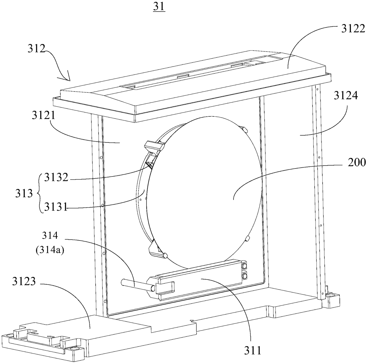
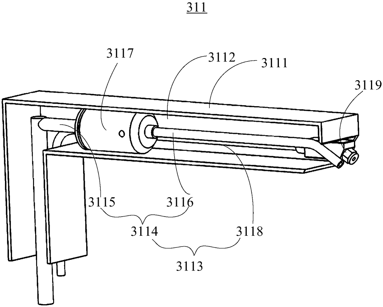
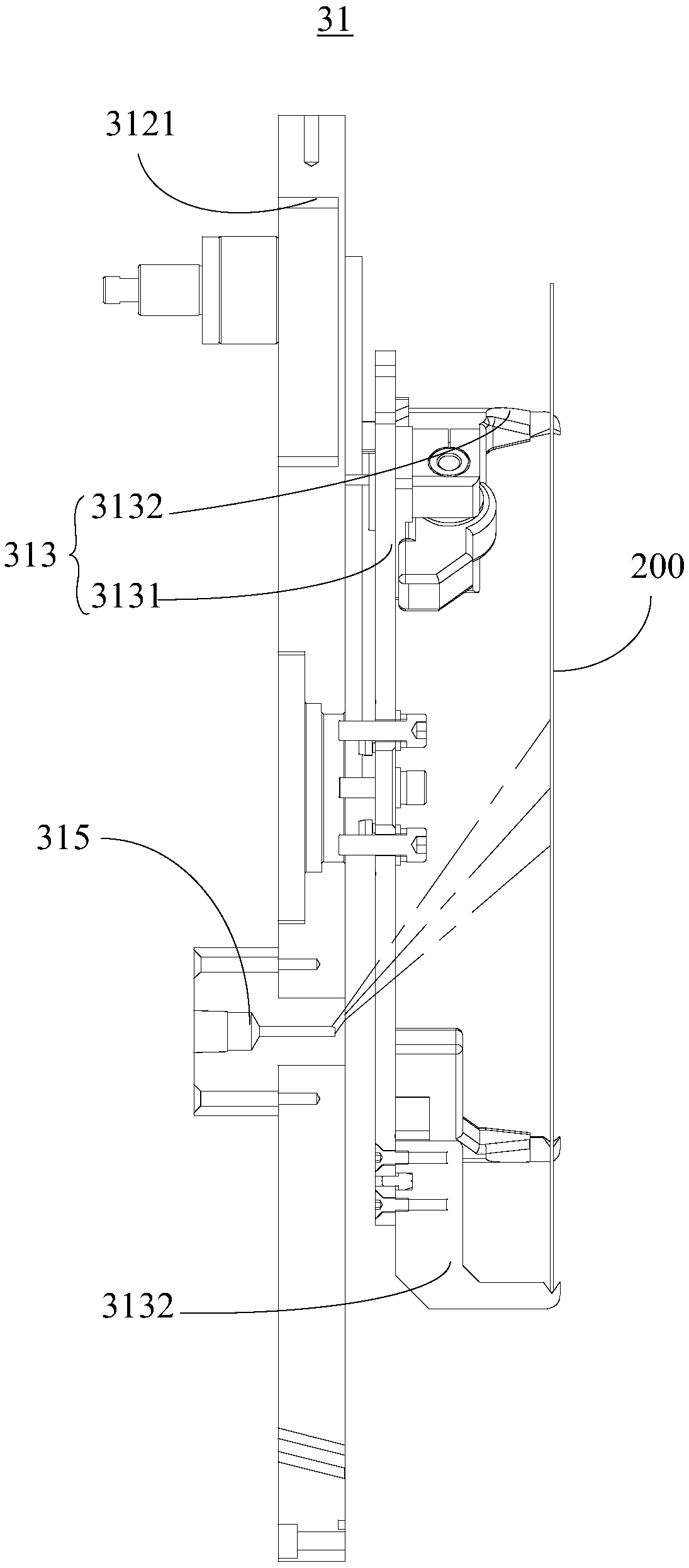
[0056] Refer below Figure 1 to Figure 9A wafer processing device 31 according to an embodiment of the first aspect of the present invention will be described. The processing device 31 of the wafer according to the embodiment of the present invention includes: a driving assembly 313 and a processing assembly 311, and the driving assembly 313 drives the wafer 200 to rotate while the processing assembly 311 swings around an axis perpendicular to the surface of the wafer 200 to move towards the wafer 200. Fluid is sprayed on the surface. ...


PUM


Abstract

The invention discloses a wafer processing device and method and a chemical mechanical polishing system. The wafer processing device comprises a driving assembly and a processing assembly, the drivingassembly drives a wafer to rotate, and the processing assembly swings around the axis perpendicular to the surface of the wafer so as to inject a fluid to the surface of the wafer. When the processing device is used for processing the wafer, the wafer can be prevented from being damaged, and the processing effect is good.

Description

technical field [0001] The invention belongs to the technical field of semiconductor technology, and in particular relates to a wafer processing device, a wafer chemical mechanical polishing system, and a wafer processing method. Background technique [0002] In the chemical mechanical polishing system in the related art, the way of cleaning the wafer will more or less cause wear or damage to the wafer, and it is easy to cause secondary pollution to the wafer and the cleaning effect is poor, so it needs to be improved. Contents of the invention [0003] The present invention aims to solve at least one of the technical problems existing in the prior art. Therefore, the present invention proposes a wafer processing device, which can prevent damage to the wafer when processing the wafer, and has a good processing effect. [0004] The invention also proposes a chemical mechanical polishing system with the wafer processing device. [0005] The present invention also proposes ...

Claims


Application Information

Patent Timeline
IPC IPC(8): B24B37/10B24B37/34H01L21/304B08B3/02B08B13/00
CPCH01L21/304B08B3/02B08B13/00B24B37/10B24B37/34
Inventor 许振杰王剑贾弘源王同庆赵德文李俊俊路新春
Owner TSINGHUA UNIV
Why Eureka
Try Eureka