Wafer and chip
A wafer and chip technology, applied in the direction of electrical components, electrical solid devices, circuits, etc., can solve problems such as optical alignment failure, wafer slide damage, wafer warpage deformation, etc., to reduce wafer warpage and improve Wafer yield, the effect of achieving stress balance
- Summary
- Abstract
- Description
- Claims
- Application Information
AI Technical Summary
Problems solved by technology
Method used
Image

Examples
Embodiment 1
[0061] In this embodiment, from the level of the wafer, by setting the gate line gaps in different directions in different regions of the wafer, the stress balance is realized and the defect of wafer warping during the wafer manufacturing process is reduced.
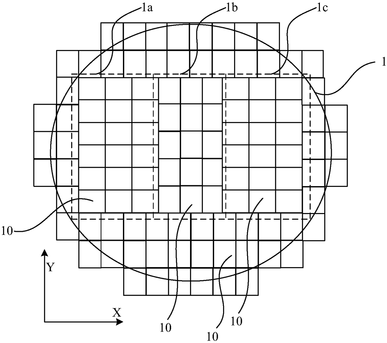
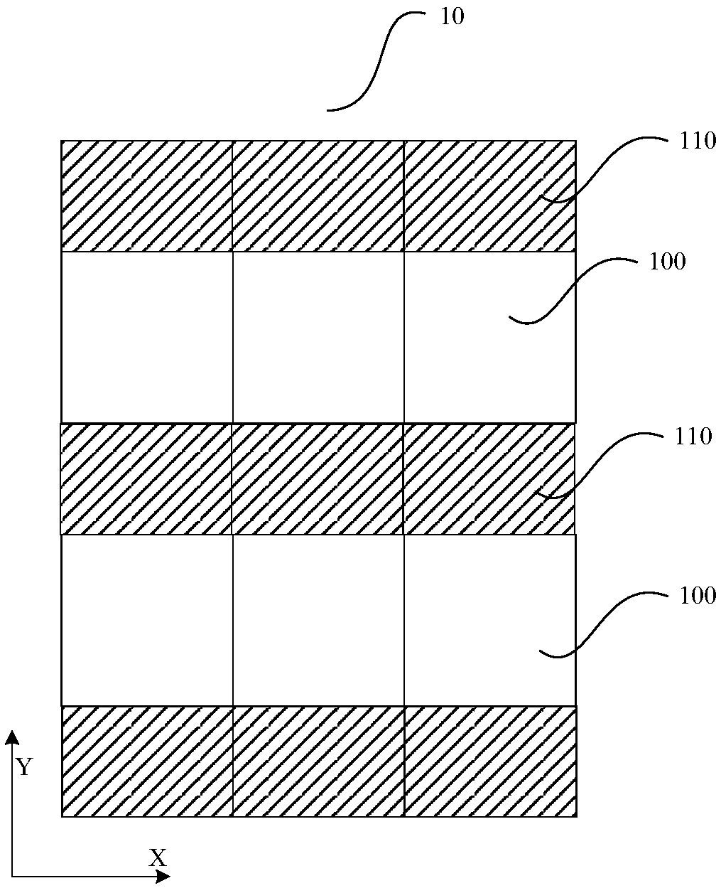
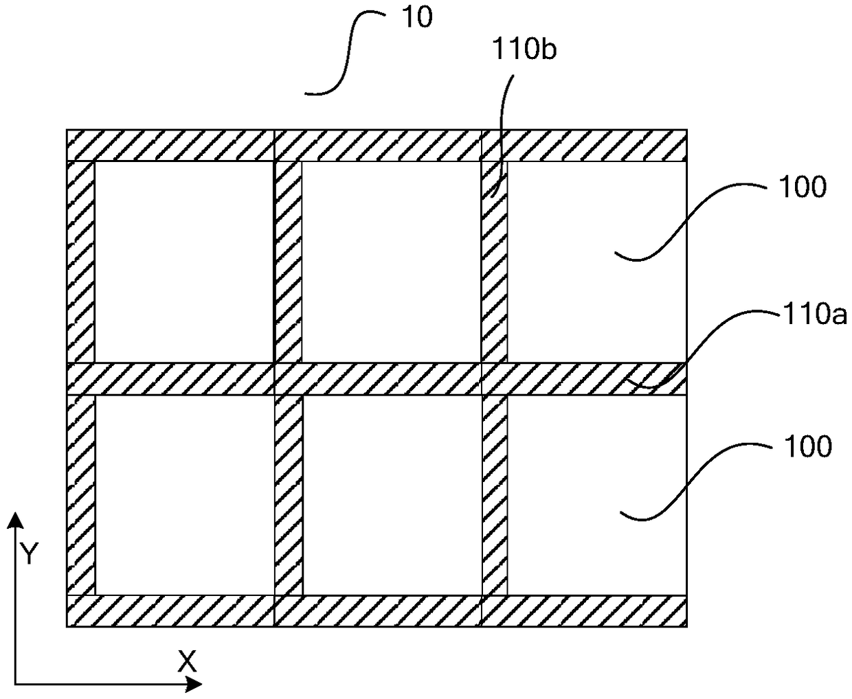
[0062] refer to Figure 1-Figure 3 As shown, among them, figure 1 is the exposure field map (shot map) of the wafer, figure 2 and image 3 It is a schematic top view of an exposure field area (shot). The wafer 1 of this embodiment includes a plurality of sub-regions 1a, 1b, and 1c, and a plurality of exposure field areas 10 are arranged in an array in each of the sub-regions 1a, 1b, and 1c. A plurality of chip areas 100 are arranged in an array in each exposure field area 10, and the exposure field area 10 is an area exposed by photolithography once in the wafer manufacturing process.
[0063] refer to Figure 4-6 As shown, the storage area of the chip area 100 includes: a stacked layer 102 located on a substrate ...
Embodiment 2
[0074] In this embodiment, from the level of the effective chip unit, by setting gate line gaps in different directions in different regions, stress balance is achieved, and the defect of wafer warpage in the wafer manufacturing process is reduced.
[0075] It can be understood that, in this application, a chip may exist on a wafer, or may be a bare chip after wafer dicing, or may be a packaged chip.
[0076] Generally, in order to increase the capacity of the chip, multiple planes are usually designed in the storage area of the chip, and each plane has basically the same capacity, that is, has basically the same number of storage units.
[0077] In this embodiment, a chip 100 is proposed, referring to Figure 7 As shown, the storage area of the chip 100 includes a plurality of areas, which are referred to as cell array areas (100a, 100b, 100c, 100d) for ease of understanding and description.
[0078] refer to Figure 7 and Figure 4 , Figure 5 As shown, the cell arra...
Embodiment 3
[0088] In this embodiment, from the plane level of the chip, the gate line gaps in different directions are set in different blocks to achieve stress balance and reduce wafer warpage in the wafer manufacturing process. Defects.
[0089] Generally, in order to increase the capacity of the chip, multiple planes are usually designed in the storage area of the chip, and each plane has basically the same capacity, that is, has basically the same number of storage units. Multiple blocks can be designed in each slice, and each block has basically the same capacity, that is, has basically the same number of storage units.
[0090] In this embodiment, a chip is proposed, refer to Figure 8 As shown, the chip area includes a plurality of block areas, which are referred to as cell array areas (1000a, 1000b, 1000c, 1000d) for ease of understanding and description.
[0091] refer to Figure 8 and Figure 4 , Figure 5 As shown, the cell array region includes: a stacked layer 102 on ...
PUM
 Abstract
Description
Claims
Application Information
 - R&D
- Intellectual Property
- Life Sciences
- Materials
- Tech Scout
- Unparalleled Data Quality
- Higher Quality Content
- 60% Fewer Hallucinations
Browse by: Latest US Patents, China's latest patents, Technical Efficacy Thesaurus, Application Domain, Technology Topic, Popular Technical Reports.
© 2025 PatSnap. All rights reserved.Legal|Privacy policy|Modern Slavery Act Transparency Statement|Sitemap|About US| Contact US: help@patsnap.com