Supercharge Your Innovation With Domain-Expert AI Agents!

Bi-directional ESD protection device of latch-up immunity

A device and latch-up technology, applied in the field of ESD protection devices, can solve the problems of reducing robustness and increasing area, and achieve the effect of improving robustness and avoiding latch-up effect

Active Publication Date: 2019-01-01
UNIV OF ELECTRONICS SCI & TECH OF CHINA
View PDF6 Cites 2 Cited by
  • Summary
  • Abstract
  • Description
  • Claims
  • Application Information

AI Technical Summary

Problems solved by technology

That is: the need for latch-free operation will reduce the robustness, and if the ESD robustness of the latch-free device needs to be improved, the area needs to be increased

Method used


Image

  • Bi-directional ESD protection device of latch-up immunity
  • Bi-directional ESD protection device of latch-up immunity
  • Bi-directional ESD protection device of latch-up immunity

Examples


Embodiment 1

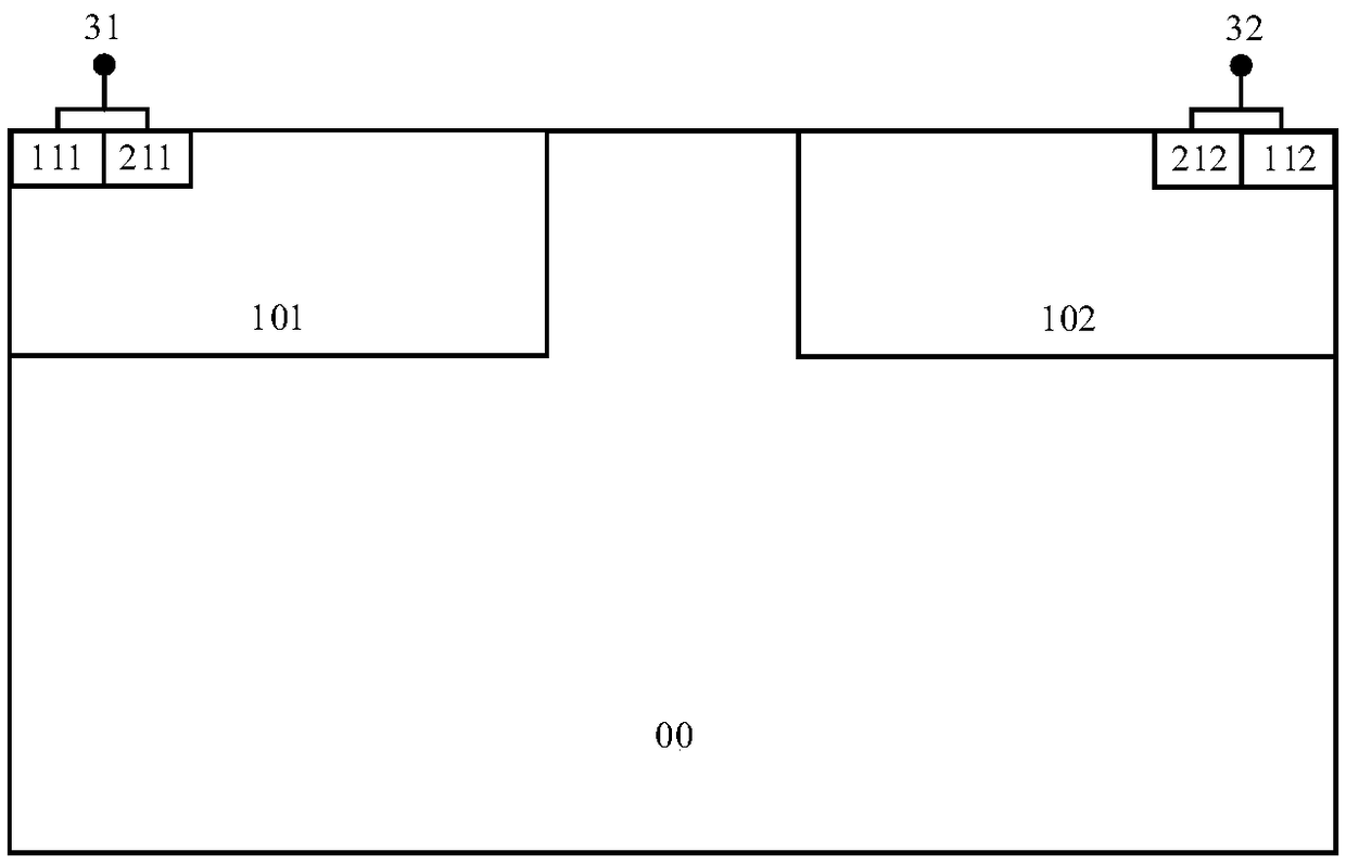
[0028] like image 3 As shown, the device structure of this embodiment includes: a P-type substrate 00, an N-type region 01 located above the P-type substrate; a first P+ contact region 211 located on the upper left side inside the N-type region 01, and The first N+ contact region 111 on the upper left side of the interior of 01, the first P+ isolation region 221 located on the upper left side of the N-type region 01, and the first P-type buried layer 231 located inside the N-type region 01; wherein, the first P+ The contact region 211 is located on the left side of the first N+ contact region 111, the first P+ isolation region 221 is located on the right side of the first N+ contact region 111, the first P-type buried layer 231 is located on the first N+ contact region 111, the first P+ contact region 211 , below the first P+ isolation region 221 and tangent to the first N+ contact region 111, the first P+ contact region 211, and the first P+ isolation region 221; the TOP lay...

Embodiment 2

[0037] like Figure 4 As shown, the difference between the device structure of this embodiment and that of Embodiment 1 is that the TOP layer 24 is a plurality of discontinuous spacer sub-regions.

Embodiment 3

[0039] like Figure 5 As shown, the difference between the device structure of this embodiment and Embodiment 1 is that: the first N+ contact region 111, the first P+ contact region 211 and the first P+ isolation region 221 form a metal anode 31 through a metal short circuit; the second N+ contact The region 112 , the second P+ contact region 212 and the second P+ isolation region 222 form a metal anode 32 by a metal short.


PUM


Abstract

The present invention provides a bi-directional ESD protection device of latch-up immunity. The device comprises: a P-type substrate, an N-type area, a first P+ contact area, a first N+ contact area,a first P+ isolation area, a first P-type buried layer and a TOP layer, a second P+ contact area, a second N+ contact area, a second P+ isolation area and a second P-type buried layer; the first N+ contact area and the first P+ contact area form a metal anode through metal short connection; the second N+ contact area and the second P+ contact area form a metal anode through metal short connection.The concentration of the P-type buried layer arranged below the P+ contact area is regulated to regulate a maintenance current so as to avoid latch-up of the device; the P-type buried layer can change the current distribution to allow an IV curve of the device to present multi-times snapback features so as to improve the robustness of the device in the ESD pulse current.

Description

technical field [0001] The invention belongs to the field of electronic science and technology, and mainly relates to the electrostatic discharge (ElectroStatic Discharge, referred to as ESD) protection technology on the integrated circuit chip, specifically relates to a class of devices with low power consumption and strong latch-up resistance. ) capability, ESD protection devices for high-voltage integrated circuits. Background technique [0002] ESD stands for Electrostatic Discharge, which is a common phenomenon in nature. ESD exists in every corner of people's daily life. But it is such a common electrical phenomenon that is a fatal threat to sophisticated integrated circuits. However, for chips that have been packaged, each power supply / input / output pin becomes a channel for pulse currents such as human body model (HBM), machine model (MM), and human body metal model (HMM). Strong ESD pulses will not only cause hard failure of the chip, but also induce various effec...

Claims


Application Information

Patent Timeline
Patent Type & Authority Applications(China)
IPC IPC(8): H01L27/02
CPCH01L27/0266
Inventor 乔明肖家木齐钊梁龙飞何林蓉梁旦业张波
Owner UNIV OF ELECTRONICS SCI & TECH OF CHINA
Features
  • R&D
  • Intellectual Property
  • Life Sciences
  • Materials
  • Tech Scout
  • Unparalleled Data Quality
  • Higher Quality Content
  • 60% Fewer Hallucinations
Learn More