A preparation method of a display substrate, a display substrate and a display screen

A technology for display substrates and display screens, which is applied in the photoengraving process of the pattern surface, opto-mechanical equipment, semiconductor/solid-state device manufacturing, etc. Effectiveness of utilization rate and reduction of production and development costs

Active Publication Date: 2019-01-04
BOE TECH GRP CO LTD +1
View PDF4 Cites 3 Cited by
  • Summary
  • Abstract
  • Description
  • Claims
  • Application Information

AI Technical Summary

Problems solved by technology

[0003] However, the above photolithography process requires that in the development process of each new product, it is necessary to design and customize a set of corresponding masks.
For products with the same overall size, even if the size of the AA (Active Area, effective display area) area is the same, but the positions of the peripheral wiring and the bonding (Bonding) area are different, it is necessary to redesign and customize a new mask
[0004] Due to the rapid replacement of touch screen products and the small quantity of single items, this puts great pressure on the production and development costs of touch screen manufacturers

Method used


Image

  • A preparation method of a display substrate, a display substrate and a display screen
  • A preparation method of a display substrate, a display substrate and a display screen
  • A preparation method of a display substrate, a display substrate and a display screen

Examples


preparation example Construction

[0059] Such as Figure 5 As shown in FIG. 2 , it is a flow chart for realizing a method for manufacturing a display substrate provided by an embodiment of the present invention. The method comprises the steps of:

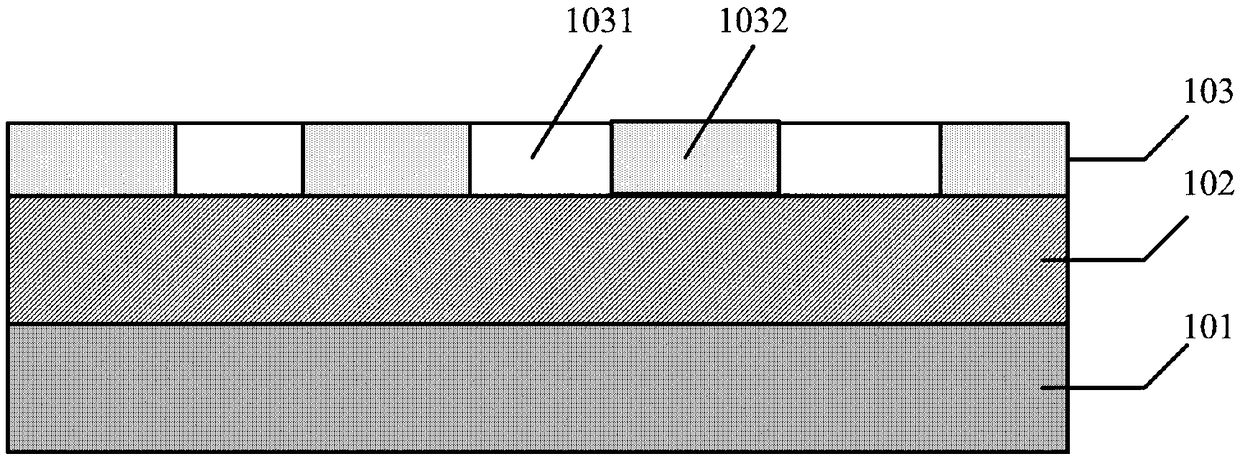
[0060] Step 50 , coating a metal material on the substrate on which the black matrix region is formed by using the first mask.

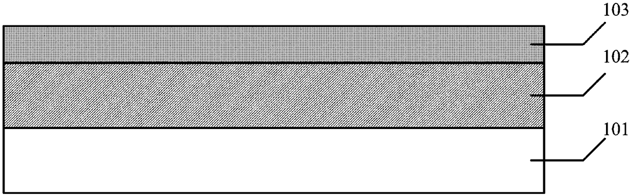
[0061] Wherein, the base substrate may be a glass substrate, a plastic substrate, or the like.

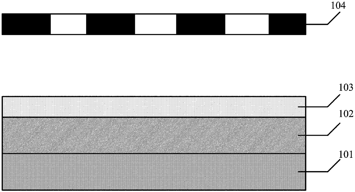
[0062] The first mask here refers to the above-mentioned BM Mask.

[0063] Step 51, coating photoresist on the metal material.

[0064] Optionally, the photoresist is a positive photoresist.

[0065] Step 52, using the second mask to perform the first exposure treatment on the photoresist.

[0066] The second mask here refers to the Metal Mask mentioned above.

[0067] Step 53, using the first mask plate to perform a second exposure treatment on the photoresist.

[0068] Step 54 , developing the photoresist after two exposures to expose pa...


PUM


Abstract

The present application discloses a preparation method of a display substrate, a display substrate and a display screen. The method includes coating a metal material on a substrate which adopts a first mask to form a black matrix region; Coating photoresist on the metal material; Performing a first exposure process on the photoresist using a second mask; Performing a second exposure process on thephotoresist by using the first mask; Developing the photoresist after two exposure treatments to expose a part of the metal material; The bare metal material is etched to form a metal layer. The technical proposal of the embodiment of the invention can improve the utilization rate of the original mask so as to reduce the production development cost.

Description

technical field [0001] The present disclosure relates to the field of display technology, in particular to a method for preparing a display substrate, a display substrate and a display screen. Background technique [0002] Due to the continuous improvement of touch precision requirements for existing touch screen products, the requirements for their production processes are gradually becoming more stringent. At present, touch screen products manufactured by photolithography processes such as mask exposure and etching can meet the performance requirements of some high-end products due to their high alignment accuracy between layers and excellent manufacturing processes of each layer. [0003] However, the above photolithography process requires that in the development process of each new product, a set of corresponding masks needs to be designed and customized. For products with the same overall size, even if their AA (Active Area, effective display area) size is the same, b...

Claims


Application Information

Patent Timeline
Patent Type & Authority Applications(China)
IPC IPC(8): H01L21/027G06F3/041
CPCG06F3/0412H01L21/0274G06F2203/04103G03F7/0005G06F3/0443G06F3/0446H10K59/40H10K71/00G06F3/04164G03F7/0041G03F7/2016
Inventor 田健许邹明张雷李亚英刘纯建郑启涛丁贤林
Owner BOE TECH GRP CO LTD
Why Eureka
Try Eureka