Integrated circuit packaging and its reflow method for improving soldering strength
A technology of integrated circuits and welding strength, applied in the direction of circuits, electrical components, electrical solid devices, etc.
- Summary
- Abstract
- Description
- Claims
- Application Information
AI Technical Summary
Problems solved by technology
Method used
Image
Examples
Embodiment 1
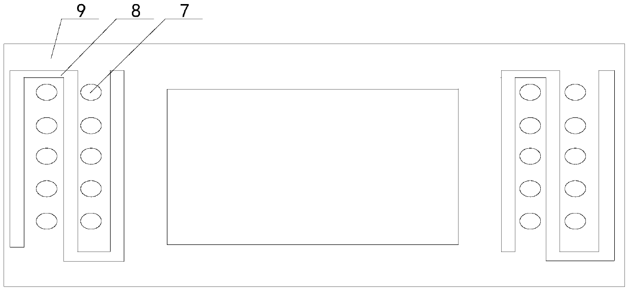
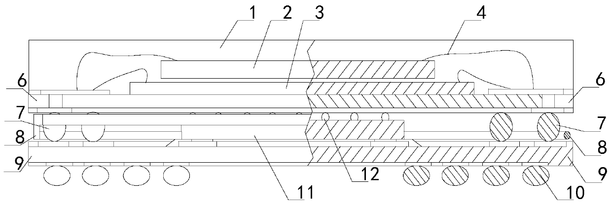
[0043] Such as figure 1 with figure 2 As shown, the integrated circuit package for improving soldering strength includes a second base 6, a second solder ball 7, an S tube 81, a first base 9, and a first chip 11, and the second base 6 is stacked on the first base 9 The upper side of the upper side, the second solder ball 7 is arranged between the second substrate 6 and the first substrate 9 so that there is no contact between the second substrate 6 and the first substrate 9; the first chip 11 is arranged between the second substrate 6 and the first substrate 9 Between the substrates 9 and flip-chip on the upper surface of the first substrate 9; there are multiple second solder balls 7, which are evenly distributed between the first substrate 9 and the second substrate 6 and form a solder ball array; the S tube 81 includes a number There are no less than three long tubes and no less than two short tubes. The long tubes and short tubes are connected at intervals to form an S s...
Embodiment 2
[0055] Such as Figure 3 to Figure 6 As shown, the difference between this embodiment and Embodiment 1 is that an internal return pipe 12 is provided on the upper side of the first chip 11, and a communication pipe is provided on the upper side of the first substrate 9, and the communication pipe and the S pipe 81 are connected end to end to form The closed outer return pipe 8 ; the contact between the inner return pipe 12 and the outer return pipe 8 enables heat transfer between the inner return pipe 12 and the outer return pipe 8 . The second chip 3 and the third chip 2 are arranged on the upper surface of the second base 6, and the second chip 3 and the third chip 2 are stacked in a naked way, and are bonded through the wire 4; in order to fix the second chip 3 and the third chip 2 are fixed together by potting glue 1 . In this embodiment, the height of the first solder ball 10 is about 0.23 mm, the thickness of the first base 9 is about 0.3 mm, the thickness of the second...
PUM
 Abstract
Description
Claims
Application Information


