Mass transfer device and related method for micro LED array device

A transfer device and device technology, applied in the direction of semiconductor devices, electrical solid devices, electrical components, etc., can solve the problems of light consumption, poor utilization of light, etc., to improve efficiency, simplify transfer methods, avoid manufacturing and removal processes Effect

Active Publication Date: 2020-11-24
XIAMEN CHANGELIGHT CO LTD
View PDF7 Cites 1 Cited by
  • Summary
  • Abstract
  • Description
  • Claims
  • Application Information

AI Technical Summary

Problems solved by technology

But the liquid crystal display will consume most of the light: from the light leaving the backlight module, passing through TFT (Thin Film Transistor, thin film transistor), liquid crystal, polarizer, color filter, and then entering the human eye, the light loss exceeds 90%. Most of the light is consumed in the display case, and the utilization rate of light is extremely poor

Method used


Image

  • Mass transfer device and related method for micro LED array device
  • Mass transfer device and related method for micro LED array device
  • Mass transfer device and related method for micro LED array device

Examples


Embodiment Construction

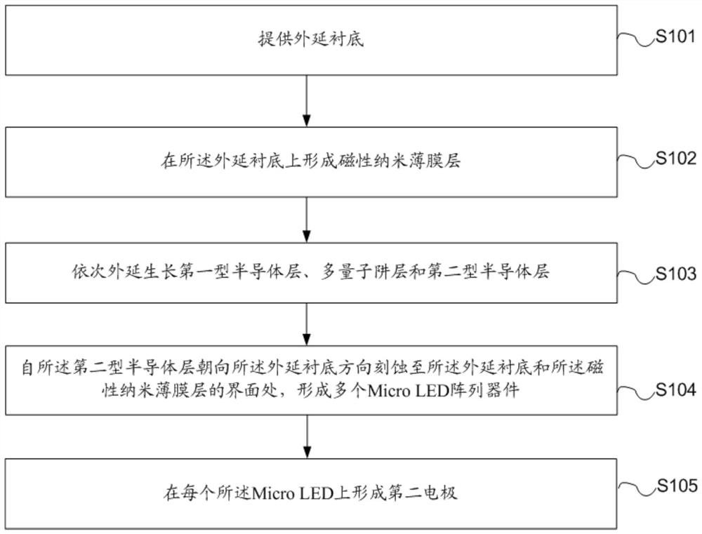
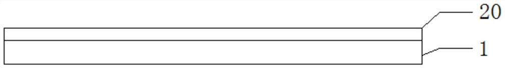
[0030] As mentioned in the background technology section, one of the difficulties in the development of Micro LED technology currently lies in the mass transfer process of Micro LED.

[0031] The inventors found that, in the prior art, methods such as bonding are provided for mass transfer, but the bonding method requires the setting of an adhesive layer and subsequent removal, which makes the process of mass transfer less efficient. Or the prior art also provides a structure in which a magnetic layer is added to the external structure of the light-emitting diode and adsorbed by magnetic force. However, since an adhesive layer is required to adhere multiple Micro LED array devices together, the adhesion needs to be removed later. The attached layer and the additional magnetic layer make the operation complicated and many steps in the mass transfer process of Micro LED array devices.

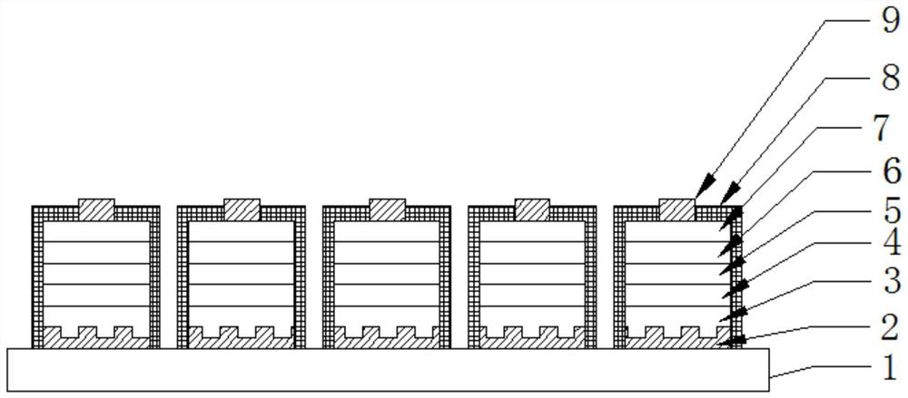
[0032] Based on this, the present invention provides a Micro LED array device, including:

...


PUM

PropertyMeasurementUnit
thicknessaaaaaaaaaa
sizeaaaaaaaaaa
diameteraaaaaaaaaa

Abstract

The invention provides a Micro LED array device and a manufacturing method thereof, A mass transfer device and a transfer method, by forming a magnetic nano-film layer on an epitaxial substrate of a Micro LED array device, As one electrode of that Micro LED array device, As a result, the Micro LED array device can be directly adsorbed by the magnetic force without adding an additional magnetic layer, the manufacturing and removing process of the magnetic layer are avoided, the transfer method of the Micro LED array device can be simplified, and the efficiency of the Micro LED mass transfer isfurther improved.

Description

technical field [0001] The present invention relates to the technical field of manufacturing semiconductor devices, in particular to a mass transfer device and a related method for a Micro LED array device. Background technique [0002] The LED (Light Emitting Diode, Light Emitting Diode) backlight display technology has been widely used in various industries. Existing LEDs are mainly used on medium and large size display screens. Taking a 55-inch 4K TV as an example, the pixel length and width are about 200 μm, and the mainstream specification of direct-lit backlight is 3030 (3mm×3mm). [0003] At present, the pixel pitch of most light-emitting diode displays is more than 100 microns. As a backlight source, the size is much larger than the pixel size and cannot be used as a point light source. High-quality full-color effects can only be achieved by using surface light sources with liquid crystals and color filters. But the liquid crystal display will consume most of the ...

Claims


Application Information

Patent Timeline
Patent Type & Authority Patents(China)
IPC IPC(8): H01L27/15H01L33/40H01L33/00
CPCH01L27/156H01L33/0095H01L33/40
Inventor 刘伟江方陈丹丹李涛彭绍文
Owner XIAMEN CHANGELIGHT CO LTD
Why Eureka
Try Eureka