
Array substrate and liquid crystal display panel

An array substrate and storage capacitor technology, applied in nonlinear optics, instruments, optics, etc., can solve the problems of low transmittance of liquid crystal display panels, low aperture ratio of pixel areas, large metal layer shading area, etc., and achieve metal shading area The effect of reducing, increasing the transmittance, and increasing the aperture ratio

Active Publication Date: 2019-01-18
CHENGDU ZHONGDIAN PANDA DISPLAY TECH CO LTD
View PDF6 Cites 7 Cited by
  • Summary
  • Abstract
  • Description
  • Claims
  • Application Information

AI Technical Summary

Problems solved by technology

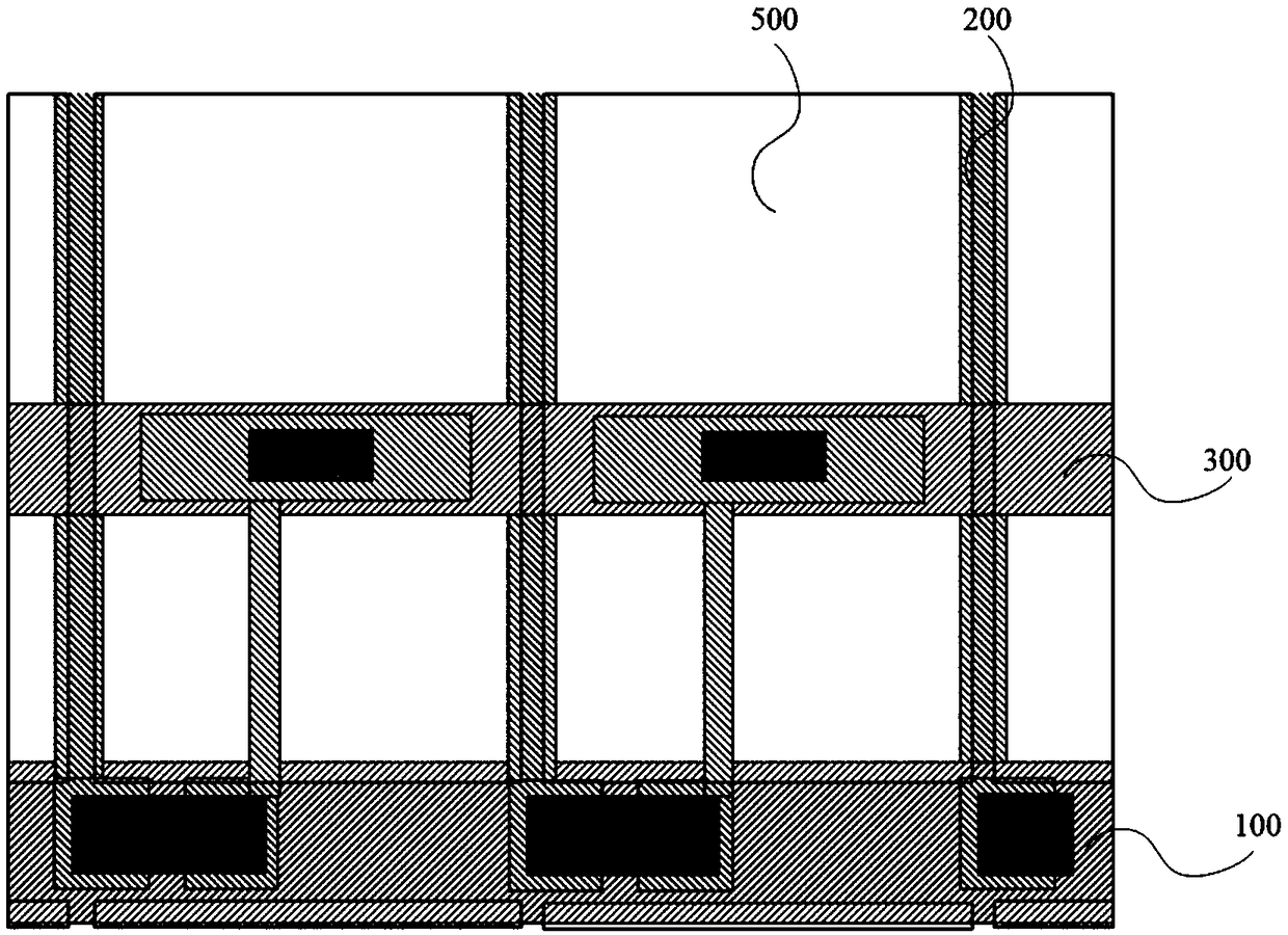
[0004] However, due to the large light-shielding area of ​​the metal layer of the storage capacitor bus 300, the aperture ratio of the pixel area is low, so the overall transmittance of the liquid crystal display panel is low.

Method used


Image

  • Array substrate and liquid crystal display panel
  • Array substrate and liquid crystal display panel

Examples


Embodiment 1

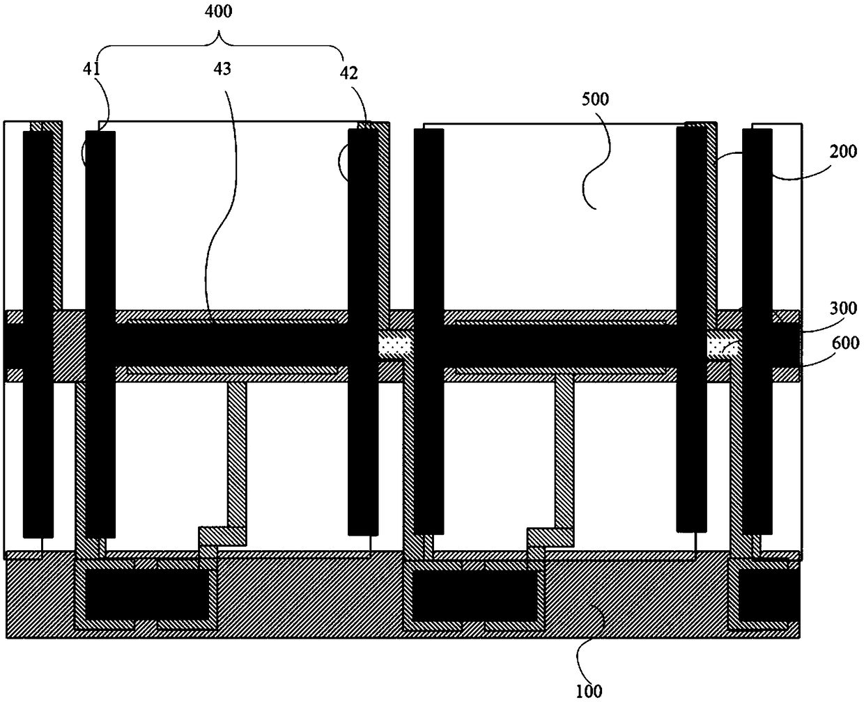
[0042] figure 2 For the circuit design diagram of the array substrate provided by the embodiment of the present invention, refer to figure 2 As shown, one aspect of the present invention provides an array substrate, including: scanning lines 100, data lines 200, storage capacitor bus lines 300, and storage capacitor branch lines 400; A pixel area 500 is formed between two adjacent scan lines 100 and two adjacent data lines 200; the storage capacitor bus 300 is arranged parallel to the scan line 100 and crosses the pixel area 500, and the storage capacitor bus 300 and the surrounding composite pixel area One of the scanning lines 100 of 500 is electrically connected; the storage capacitor branch line 400 includes a first segment 41 parallel to the data line 200, and the first segment 41 is arranged on the inner side of one of the two adjacent data lines 200 surrounding the composite pixel area 500 , the storage capacitor branch line 400 is electrically connected to the stora...

Embodiment 2

[0061] An embodiment of the present invention also provides a liquid crystal display panel, including: the array substrate as described in the above embodiment, a color filter substrate disposed opposite to the array substrate, and a color filter substrate sandwiched between the array substrate and the color filter substrate layer of liquid crystal molecules.

[0062] The general structure of a liquid crystal display panel includes a polarizer, a color filter substrate, a liquid crystal layer, an array substrate, and a polarizer arranged sequentially from top to bottom. Among them, the function of the polarizer is to control the light of the backlight to only let the light in a specific direction pass through, and filter out the light in other directions. The light processed by the polarizing plate can control the brightness of the light exiting the display screen through the twisting action of the liquid crystal molecules, thereby controlling the brightness of the light exiti...


PUM


Abstract

The invention provides an array substrate and a liquid crystal display panel. The array substrate comprises scanning lines, data lines, a storage capacitance bus and storage capacitance branches; themultiple scanning lines and the multiple data lines are arranged in a crisscrossed manner; furthermore, adjacent two scanning lines and adjacent two data lines form a pixel area in an encircling manner; the storage capacitance bus is arranged to be parallel to the scanning lines, and stretches across the pixel area; furthermore, the storage capacitance bus is electrically connected with one scanning line forming the pixel area in the encircling manner; the storage capacitance branches include a first section parallel to the data lines; furthermore, the first section is arranged at the inner side of one of adjacent two data lines forming the pixel area in the encircling manner; the storage capacitance branches are electrically connected with the storage capacitance bus; and furthermore, thestorage capacitance branches are made of a conductive transparent material. According to the array substrate and the liquid crystal display panel provided in the invention, due to arrangement of thestorage capacitance braches made of the conductive transparent material, the pixel transmittance can be effectively improved.

Description

technical field [0001] The invention relates to the field of liquid crystal display, in particular to an array substrate and a liquid crystal display panel. Background technique [0002] The transmittance of the liquid crystal display panel plays an extremely important role in the overall display performance of the liquid crystal display panel. The higher the transmittance, the higher the display brightness of the liquid crystal display panel, and the lower the brightness of the backlight source. To reduce product costs, the industry has been working hard to increase the transmittance of liquid crystal display panels. [0003] figure 1 For the circuit design diagram of the array substrate provided in the prior art, refer to figure 1 As shown, the array substrate in the conventional liquid crystal display panel includes scanning lines 100 and data lines 200 arranged vertically and horizontally, and two adjacent scanning lines 100 and two adjacent data lines 200 enclose a pl...

Claims


Application Information

Patent Timeline
Patent Type & Authority Applications(China)
IPC IPC(8): G02F1/1362G02F1/1337
CPCG02F1/1337G02F1/136213G02F1/136227G02F1/136286
Inventor 陈盈惠杨桂冬储周硕日比野吉高孙学军
Owner CHENGDU ZHONGDIAN PANDA DISPLAY TECH CO LTD
Learn More