
COB display screen and packaging method thereof

A display and PCB board technology, applied in the field of COB display and its packaging, can solve the problems of blurred luminous granular luminescence, poor consistency of physical characteristics of luminous surface, small visible surface of COB display, etc., to improve black and white contrast ratio and clarity, reducing scrap rate and improving service life

Inactive Publication Date: 2019-01-22
深圳市海讯高科技术有限公司
View PDF18 Cites 5 Cited by
  • Summary
  • Abstract
  • Description
  • Claims
  • Application Information

AI Technical Summary

Problems solved by technology

[0004] Traditional COB display screens have inherent defects such as cross-lighting, color cast, luminous granularity or luminous confusion, poor black-and-white contrast, poor consistency of physical characteristics of the luminous surface, and poor consistency of brightness and color.
[0005] The traditional COB packaging method is to paste the light-emitting chip on the PCB and fix it with silver glue. However, since the light-emitting chip cannot be completely on the same horizontal line (there will always be some deviation), there is no isolation between pixels, and the two There is mutual interference between the two light spots. The COB display screen packaged in this packaging method has the problems of small visible area, poor black-and-white contrast, cross-light and color cast.

Method used


Image

  • COB display screen and packaging method thereof
  • COB display screen and packaging method thereof
  • COB display screen and packaging method thereof

Examples


Embodiment Construction

[0036] The following will clearly and completely describe the technical solutions in the embodiments of the present invention with reference to the accompanying drawings in the embodiments of the present invention. Obviously, the described embodiments are only some, not all, embodiments of the present invention. Based on the embodiments of the present invention, all other embodiments obtained by persons of ordinary skill in the art without making creative efforts belong to the protection scope of the present invention.

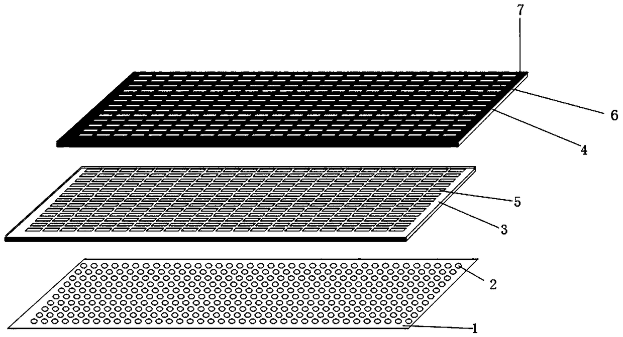
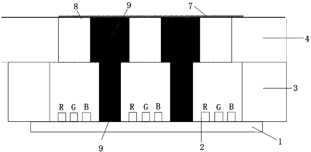
[0037] see figure 1 and figure 2 , in an embodiment of the present invention, a COB display screen includes a PCB board 1, a first mask 3 and a second mask 4, a plurality of light-emitting chips 2 are mounted equidistantly on the plane of the PCB board 1, and the light-emitting chips 2 It is fixed on the PCB board 1 by silver glue.

[0038] The first mask 3 is covered on the PCB board 1, and the second mask 4 is covered on the first mask 3. Both the first m...


PUM


Abstract

The invention discloses a COB display screen and a packaging method of the COB display screen. The COB display screen comprises a PCB, a first face cover and a second face cover, wherein a plurality of light-emitting chips are mounted on the upper plane of the PCB at equal intervals, and the light-emitting chips are fixed to the PCB through silver colloid. The PCB is covered by the first face cover, the first face cover is covered by the second face cover, a plurality of first face cover holes are arranged in the first face cover, a plurality of second face cover holes are arranged in the second face cover, the first face cover holes and the second face cover holes are in one-to-one correspondence and are positioned on the same axial line, the inner diameters of the second face cover holesare smaller than those of the first face cover holes, the peripheral surfaces of the first face cover holes are subjected to mirror surface treatment, the peripheral surfaces of the second face coverholes are subjected to frosting treatment, and the heights of the first face cover holes are greater than the widths of the first face cover holes. For the COB display screen and the packaging methodof the COB display screen, through the light refraction, the light mixing is uniform, meanwhile, light is emitted in the diffuse reflection manner, so that the mixed color of the scattered light is little, the visual surface is large, thus the black and white contrast of the display screen is improved, dazzle light is reduced, and then the luminance of the light is more uniform.

Description

technical field [0001] The invention relates to the field of COB display screens, in particular to a COB display screen and a packaging method thereof. Background technique [0002] At present, the LED full-color display is to package the LED red, green and blue chips into SMD devices, and then paste them on the PCB through printing, patch, reflow soldering and other methods to form an LED module display. The LED lamp beads used in the modules above P2 are SMD devices made by packaging the chip on the bracket, mainly through die bonding, wire bonding, dispensing, light splitting, tape, and packaging. [0003] COB technology is an emerging LED packaging technology, which is different from traditional SMD surface-mount packaging. It integrates light-emitting chips into the PCB board instead of soldering them to the PCB one by one. COB technology effectively improves the light color of the LED display, reduces risks and costs. [0004] Traditional COB display screens have inh...

Claims


Application Information

Patent Timeline
Patent Type & Authority Applications(China)
IPC IPC(8): G09F9/33
CPCG09F9/33
Inventor 田国辉
Owner 深圳市海讯高科技术有限公司
Learn More