Mini LED module and a manufacturing method thereof

A manufacturing method and module technology, which is applied in the fields of printed circuit manufacturing, printed circuit assembled with electrical components, printed circuit connected with non-printed electrical components, etc., can solve the problem of reducing the placement yield of Mini LED modules and increasing the number of Mini LED chips Difficulty in placement, large cumulative tolerance and other issues, to achieve the effect of reducing cumulative tolerance, avoiding offset, and improving placement yield

Pending Publication Date: 2019-01-22
APT ELECTRONICS
View PDF0 Cites 6 Cited by
  • Summary
  • Abstract
  • Description
  • Claims
  • Application Information

AI Technical Summary

Problems solved by technology

However, on the one hand, since the size of flip-chip Mini LED chips is tens of microns and the size of conventional LED chips is submillimeter, the size of flip-chip Mini LED chips is much smaller than that of conventional LED chips, and flip-chip The pad diameter of the mini LED chip is less than 150μm, which is generally only 1 / 10 of the pad diameter of the conventional LED chip, which makes it easy to reduce the size of the Mini LED module due to the offset of the Mini LED chip when making the Mini LED module. Mounting yield
[0004] On the other hand, due to the limitation of the PCB board manufacturing process, the diameter of the pads of the existing PCB boards is greater than 150 μm; and when preparing the Mini LED module, a PCB board is usually provided with multiple pads distributed in an array. Make the PCB board have a larger size
Therefore, the existing Mini LED modules still have large cumulative tolerances due to the large size of the PCB, which increases the difficulty of mounting Mini LED chips on large-size PCBs, thereby reducing the placement yield of Mini LED modules.

Method used


Image

  • Mini LED module and a manufacturing method thereof
  • Mini LED module and a manufacturing method thereof
  • Mini LED module and a manufacturing method thereof

Examples


Embodiment 1

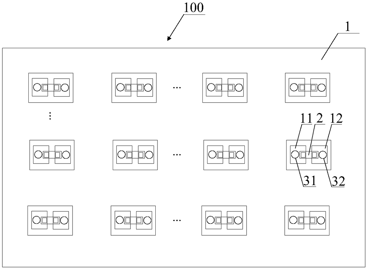
[0047] See figure 1 , is a schematic structural diagram of a Mini LED module according to Embodiment 1 of the present invention.

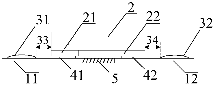
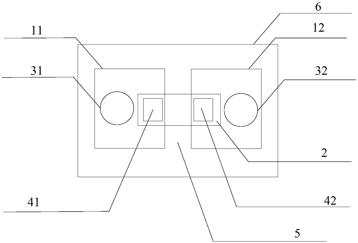
[0048] Such as figure 1 and figure 2 As shown, the Mini LED module 100 includes: a PCB board 1 and at least one Mini LED chip 2; at least one group of component pads is provided on the PCB board 1, and at least one group of component pads includes the first pad 11 and The second pad 12, the first pad 11 is provided with a first solder resist point 31, and the second pad 12 is provided with a second solder resist point 32, so as to locate the installation position of at least one Mini LED chip 2; The anode pad 21 of the at least one Mini LED chip 2 is connected to the first pad 11, and the cathode pad 22 of the at least one Mini LED chip 2 is connected to the second pad 12; the at least one Mini LED chip 2 is located at the first There is a first gap 33 between the solder resist point 31 and the second solder resist point 32, and between the at ...

Embodiment 2

[0069] See Figure 6 , is a schematic flowchart of a manufacturing method of a Mini LED module according to Embodiment 2 of the present invention.

[0070] Such as Figure 6 and Figure 7 As shown in the schematic diagram of steps 7a to 7d, the manufacturing method of the Mini LED module is suitable for manufacturing at least one Mini LED chip on at least one group of component pads on the PCB, including the following steps:

[0071] S1. According to the preset glue dispensing position, make a first solder resist point on the first pad of at least one group of component pads, and make a second solder resist point on the second pad of at least one group of component pads, To locate the mounting position of at least one Mini LED chip;

[0072] Wherein, in step S1, the dispensing positions of the first solder resist point and the second solder resist point are determined through the following steps:

[0073] S11. Pre-dotting a first solder resist point on the first pad and pr...


PUM


Abstract

The invention discloses a Mini LED module and a manufacturing method thereof. The Mini LED module comprises a PCB board and at least one Mini LED chip. The first pad on the PCB is provided with a first solder resist, and the second pad is provided with a second solder resist. The positive electrode pad of the Mini LED chip is connected with the first pad, and the negative electrode pad of the MiniLED chip is connected with the second pad. The Mini LED chip is positioned between the first solder resist and the second solder resist, and has a first gap between the Mini LED chip and the first solder resist, and a second gap between the Mini LED chip and the second solder resist. The Mini LED module and the manufacturing method thereof can effectively improve the mounting yield of the Mini LED chip and reduce the accumulated tolerance of the Mini LED chip mounted on the large-size PCB board.

Description

technical field [0001] The invention relates to the technical field of LEDs, in particular to a Mini LED module and a manufacturing method thereof. Background technique [0002] Mini LED chip is a kind of LED chip with a chip size of about 100μm×100μm. It has the advantages of high color saturation, local dimming, high brightness, and energy saving. It can be applied to backlight displays and has become a recent research hotspot. [0003] In order to improve the color rendering of the backlight display, the existing Mini LED modules usually mount the Mini LED chip on the PCB to achieve an ultra-small light mixing distance. However, on the one hand, since the size of flip-chip Mini LED chips is tens of microns and the size of conventional LED chips is submillimeter, the size of flip-chip Mini LED chips is much smaller than that of conventional LED chips, and flip-chip The pad diameter of the mini LED chip is less than 150μm, which is generally only 1 / 10 of the pad diameter o...

Claims


Application Information

Patent Timeline
Patent Type & Authority Applications(China)
IPC IPC(8): H05K1/11H05K1/18H05K3/34H01L25/075H01L33/62
CPCH05K1/111H01L25/0753H01L33/62H05K1/181H05K3/341H05K2201/09427
Inventor 曾照明姚述光刘德武万垂铭区伟能邝健
Owner APT ELECTRONICS
Why Eureka
Try Eureka