A chip package structure and method

A technology of chip packaging structure and shielding structure, which is applied in the electronic field, can solve problems such as unreliable chip safety performance and system shutdown, and achieve the effects of improving use safety, improving heat dissipation performance, and ensuring work stability

Pending Publication Date: 2019-01-25
中国科学院苏州纳米技术与纳米仿生研究所南昌研究院
View PDF6 Cites 2 Cited by
  • Summary
  • Abstract
  • Description
  • Claims
  • Application Information

AI Technical Summary

Problems solved by technology

When the system is running at full capacity, if the chip cannot dissipate heat in time or the safety performance is unreliable, the relevant system will shut down, and in severe cases, it will cause immeasurable consequences

Method used


Image

  • A chip package structure and method
  • A chip package structure and method
  • A chip package structure and method

Examples


Embodiment Construction

[0022] In view of the deficiencies in the prior art, the inventor of this case was able to propose the technical solution of the present invention after long-term research and extensive practice. The technical solution, its implementation process and principle will be further explained as follows.

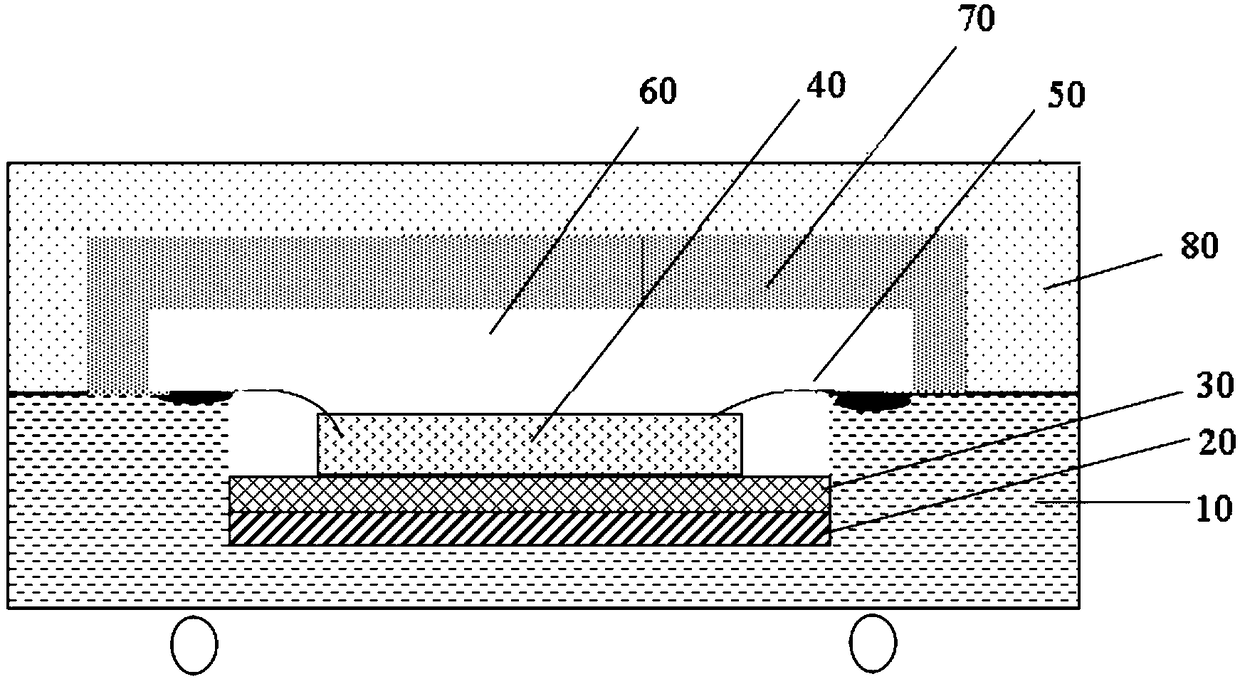
[0023] A chip packaging structure provided by an embodiment of the present invention includes:

[0024] Substrate;

[0025] a heat dissipation layer arranged on one side surface of the substrate;

[0026] a wafer, disposed on a side of the heat dissipation layer away from the substrate;

[0027] The shielding structure is fixedly installed on the substrate and covers the periphery of the wafer, and a cavity is formed between the shielding structure and the wafer.

[0028] In some embodiments, the heat dissipation layer includes a heat conduction layer and an adhesive layer, and the wafer is connected to the heat conduction layer through the adhesive layer.

[0029] In some pref...


PUM


Abstract

The invention discloses a chip packaging structure, comprising: a substrate; A heat dissipation layer arranged on one side surface of the substrate; A wafer disposed on a side of the heat dissipationlayer remote from the substrate; The shielding structure is fixedly mounted on the substrate and covers the periphery of the wafer, and a cavity is formed between the shielding structure and the wafer. The chip packaging structure of the invention has good heat dissipation performance, safety and reliability. At that same time, by provide a shielding structure, which can not only protect the circuit structure on the surface of the wafer, At the same time, the shielding structure has the ability of anti-electromagnetic interference, which can effectively prevent the chip packaging structure from being disturbed by electromagnetic waves in the work, ensure the stability of the control system of the chip packaging structure, and improve the use safety of the chip packaging structure.

Description

technical field [0001] The invention relates to the field of electronic technology, in particular to a chip packaging structure and method. Background technique [0002] Due to the rapid development of the semiconductor industry, the power consumption of semiconductor chips continues to increase in order to meet system requirements, and heat dissipation becomes more and more difficult. At the same time, as the semiconductor industry has risen to a national strategic level, new challenges have been raised to the security performance of chips. At present, chip heat dissipation and safety performance determine the reliability of the chip. When the system is running at full capacity, if the chip cannot dissipate heat in time or the safety performance is unreliable, the related system will shut down, and in severe cases, it will cause immeasurable consequences. Contents of the invention [0003] The main purpose of the present invention is to provide a chip packaging structur...

Claims


Application Information

Patent Timeline
Patent Type & Authority Applications(China)
IPC IPC(8): H01L23/31H01L23/367H01L23/552
CPCH01L23/552H01L23/31H01L23/367
Inventor 范亚明朱璞成刘斌
Owner 中国科学院苏州纳米技术与纳米仿生研究所南昌研究院
Why Eureka
Try Eureka