Structure for realizing the nested connection of an antenna and a circuit

An antenna and circuit technology, which is applied in the field of nested connection between antenna and circuit, can solve the problems of high dielectric constant, low gain, large connection loss between antenna and chip circuit, etc., to suppress surface waves, improve antenna gain, Inhibition of intensive effects

Inactive Publication Date: 2019-01-25
BEIJING UNIV OF POSTS & TELECOMM
View PDF2 Cites 7 Cited by
  • Summary
  • Abstract
  • Description
  • Claims
  • Application Information

AI Technical Summary

Problems solved by technology

However, the medium of these processes has high dielectric loss and high dielectric constant, which causes the antenna to generate large surface waves, resulting in narrow antenna bandwidth, low radiation efficiency (<10%), low gain (less than -10dBi), and reduced radiation lobe.
Secondly, due to the short millimeter wave / terahertz wavelength, the size of the antenna can be compared with the size of the chip. Therefore, the antenna and the chip circuit can be integrated together, but there are problems such as large connection loss between the antenna and the chip circuit, and coupling interaction.
At present, the main methods of suppressing the surface of millimeter-wave / terahertz antennas are slotting silicon-based dielectrics, loading dielectrics and metamaterials on the surface of chip antennas, but these methods all introduce more complex structures and processing techniques

Method used


Image

  • Structure for realizing the nested connection of an antenna and a circuit
  • Structure for realizing the nested connection of an antenna and a circuit
  • Structure for realizing the nested connection of an antenna and a circuit

Examples


Embodiment Construction

[0024] In order to make the object, technical solution and advantages of the present invention clearer, the present invention will be described in further detail below in conjunction with specific embodiments and with reference to the accompanying drawings.

[0025] It should be noted that all expressions using "first" and "second" in the embodiments of the present invention are to distinguish two entities with the same name but different parameters or parameters that are not the same, see "first" and "second" It is only for the convenience of expression, and should not be construed as a limitation on the embodiments of the present invention, which will not be described one by one in the subsequent embodiments.

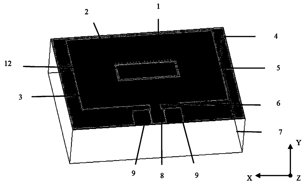
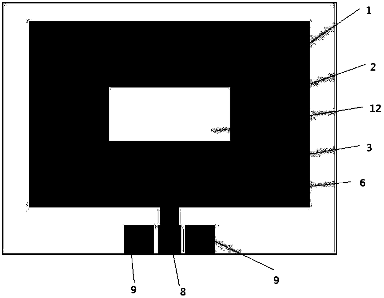
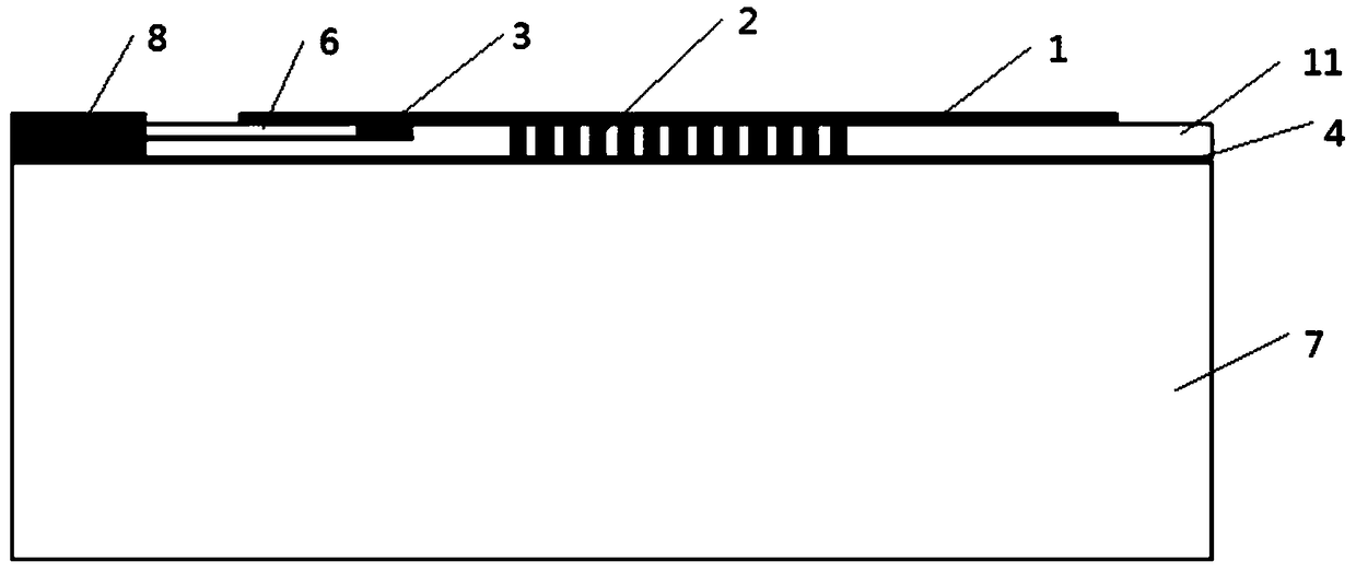
[0026] figure 1 It is a perspective view of a structure that realizes the nested connection between the antenna and the circuit according to the embodiment of the present invention; figure 2 It is a top view of a structure that realizes the nested connection between...


PUM


Abstract

The invention discloses a structure for realizing the nesting connection of an antenna and a circuit, which comprises a suppression surface wave antenna, a chip circuit and a coplanar waveguide pad. The suppression surface wave antenna comprises a feeding probe and a silicon substrate, a metal floor, a dielectric layer and a radiation patch layered from bottom to top. A short-circuit concentric ring is arranged on the radiation patch, and the short-circuit concentric ring is concentrically arranged with the radiation patch, and the radiation patch is connected with the metal floor through theshort-circuit concentric ring; The radiation patch part located inside the short-circuit concentric ring is provided with a slot for placing the chip circuit. One end of the feeding probe is connectedwith a radiation patch; The coplanar waveguide pad includes a ground plane disposed on a metal ground plane and a signal line connected to the other end of the feed probe.

Description

technical field [0001] The invention relates to the technical field of antennas, in particular to a structure for realizing nested connection between antennas and circuits. Background technique [0002] With people's continuous exploration of the electromagnetic spectrum, millimeter wave / terahertz (0.1THz-10THz) can effectively solve the problem of wireless access due to its rich spectrum resources, short wavelength, low interference, and the ability to achieve a data transmission rate of Gbps. Many problems it faces have broad application prospects in broadband wireless communication and imaging systems. With the advancement of solid-state electronic technology, millimeter-wave / terahertz chip circuits have gradually developed. Through integrated electronic devices, up-conversion from microwave signals to millimeter-wave / terahertz has become a low-cost, highly integrated millimeter-wave / terahertz system. the best way. [0003] In the past ten years, the commonly used milli...

Claims


Application Information

Patent Timeline
Patent Type & Authority Applications(China)
IPC IPC(8): H01Q1/38H01Q1/48H01Q1/50H01Q1/52H01Q1/22
CPCH01Q1/38H01Q1/2283H01Q1/48H01Q1/50H01Q1/52
Inventor 朱华李秀萍
Owner BEIJING UNIV OF POSTS & TELECOMM
Why Eureka
Try Eureka