Semiconductor device structure and formation method thereof

A device structure and semiconductor technology, applied in semiconductor devices, semiconductor/solid-state device manufacturing, electrical components, etc., can solve the problems of poor device performance and difficult control, and achieve the effect of accurately controlling the channel length and improving performance

Inactive Publication Date: 2019-01-29
SHANGHAI ZHUANXIN CORP MANAGEMENT CONSULTING PARTNERSHIP LLP
View PDF0 Cites 0 Cited by
  • Summary
  • Abstract
  • Description
  • Claims
  • Application Information

AI Technical Summary

Problems solved by technology

However, these methods are difficult to control in actual production, resulting in poor device performance

Method used


Image

  • Semiconductor device structure and formation method thereof
  • Semiconductor device structure and formation method thereof
  • Semiconductor device structure and formation method thereof

Examples


Embodiment Construction

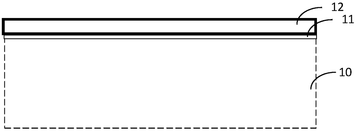
[0032] Various exemplary embodiments, features, and aspects of the present disclosure will be described in detail below with reference to the drawings. The same reference signs in the drawings indicate elements with the same or similar functions. Although various aspects of the embodiments are shown in the drawings, unless otherwise noted, the drawings are not necessarily drawn to scale.

[0033] The dedicated word "exemplary" here means "serving as an example, embodiment, or illustration." Any embodiment described herein as "exemplary" need not be construed as being superior or better than other embodiments.

[0034] In addition, in order to better illustrate the present disclosure, numerous specific details are given in the following specific embodiments. Those skilled in the art should understand that without certain specific details, the present disclosure can also be implemented. In some instances, the methods, means, elements, and circuits well-known to those skilled in th...


PUM


Abstract

The invention relates to a semiconductor device structure and a formation method thereof. The formation method comprises the steps of successively forming a first dielectric layer, a second dielectriclayer and a third dielectric layer on a substrate; etching the third dielectric layer and the second dielectric layer in sequence to form a first implantation region; carrying out first ion implantation processing on the first implantation region to form a doping region in the substrate; carrying out oxidization processing on the second dielectric layer according to a thermal oxidization method to generate a fourth dielectric layer around the second dielectric layer, and forming a second implantation region; and carrying out second ion implantation processing on the second ion implantation region, and forming a source region of the semiconductor device is formed in the substrate. The channel length of the device can be accurately controlled through accurately controlling the source region, and the performance of the MOS device is improved.

Description

Technical field [0001] The present disclosure relates to the field of semiconductor process technology, and in particular to a semiconductor device structure and a method of forming the same. Background technique [0002] In high-voltage and high-current semiconductor devices (such as vertical double diffused metal oxide transistors VDMOS and laterally diffused metal oxide transistors LDMOS), a doped body region needs to be formed between the gate and the source to make the device in When a voltage is applied, a channel is formed and turned on. In related technologies, ion implantation and high-temperature annealing are usually used to achieve impurity diffusion, or large-angle ion implantation is used for doping. However, these methods are difficult to control in actual production, resulting in poor device performance. Summary of the invention [0003] In view of this, the present disclosure proposes a semiconductor device structure and a forming method thereof, which can obtai...

Claims


Application Information

Patent Timeline
Patent Type & Authority Applications(China)
IPC IPC(8): H01L21/336H01L29/78
CPCH01L29/66674H01L29/7801
Inventor 黄海涛张永熙陈伟
Owner SHANGHAI ZHUANXIN CORP MANAGEMENT CONSULTING PARTNERSHIP LLP
Why Eureka
Try Eureka