Method of forming light doped drain electrode using side wall polymer grid structure

A lightly doped drain and gate structure technology, applied in electrical components, semiconductor/solid-state device manufacturing, circuits, etc., can solve problems such as difficulty in manufacturing, lower component yield and electrical quality, and affect component stability

Inactive Publication Date: 2006-06-14
GRACE SEMICON MFG CORP
View PDF0 Cites 0 Cited by
  • Summary
  • Abstract
  • Description
  • Claims
  • Application Information

AI Technical Summary

Problems solved by technology

[0004] However, in the subsequent thermal process of the LDD24, the ions of the LDD24 are often diffused laterally due to heating, such as Figure 1C As shown, the diffusion to the position below the polysilicon gate 14 invades the channel region and shortens the length of the channel. This phenomenon will cause leakage current, punch through effect and shallow polysilicon gate. Short channel effects such as parasitic capacitors in ion-doped regions, this short channel effect is particularly significant in sub-micron processes (less than 0.15μm process)
[0005] Therefore, in the face of higher and higher integration of components and smaller and smaller process line widths, the lateral diffusion of LDD caused by subsequent thermal processes will not only shorten the channel distance, but will further form short trenches of components. The channel effect will affect the stability of components, making it difficult to make smaller semiconductor components, reducing the yield and electrical quality of components

Method used


Image

  • Method of forming light doped drain electrode using side wall polymer grid structure
  • Method of forming light doped drain electrode using side wall polymer grid structure
  • Method of forming light doped drain electrode using side wall polymer grid structure

Examples


Embodiment Construction

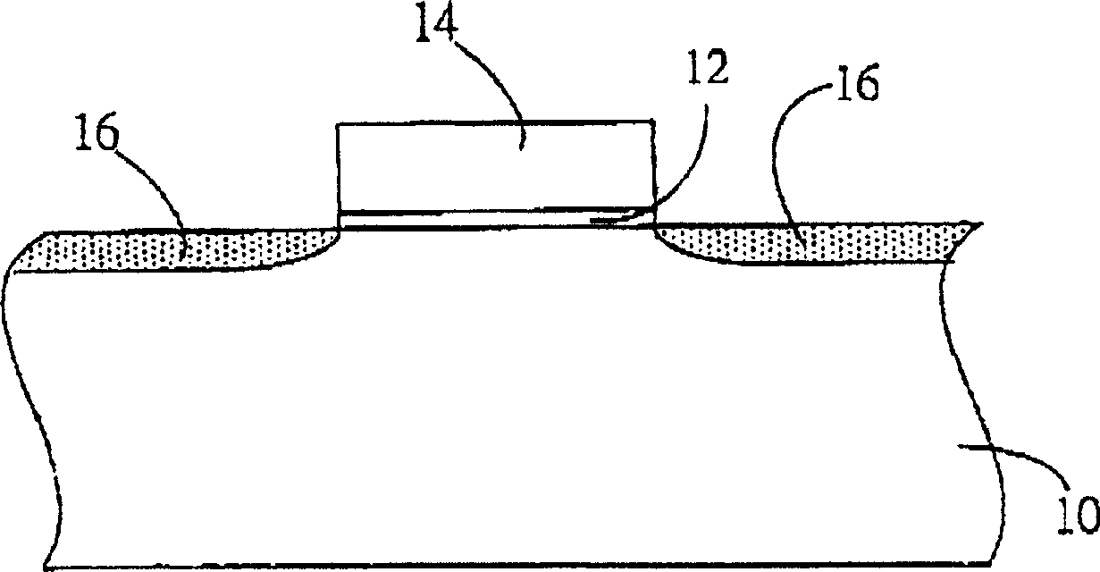
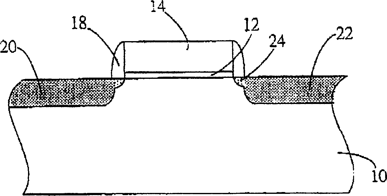
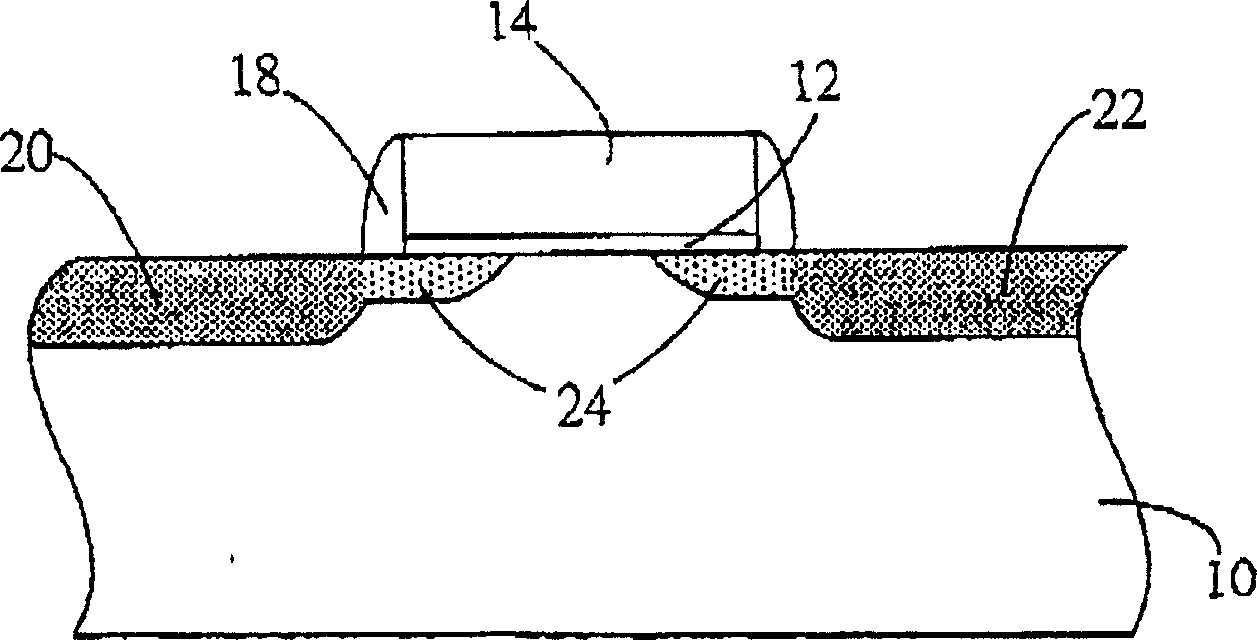
[0013] The present invention is a sidewall polymer (sidewall) pre-formed on the substrate, so that after the shallow ion doping area is formed, the shallow ion doping area only diffuses laterally to the substrate under the sidewall polymer during thermal processing When forming the LDD structure, the length of the channel can be accurately controlled, effectively solving the common short channel effect in the semiconductor process.

[0014] Figure 2A to Figure 2F These are schematic cross-sectional schematic diagrams of each step of manufacturing LDD in a preferred embodiment of the present invention; as shown in the figure, the manufacturing method of the present invention includes the following steps:

[0015] First, see Figure 2A As shown, a gate oxide layer 22 is formed by thermal oxidation on a substrate 20; then, a polysilicon layer 24 is deposited on the gate oxide layer 22 by chemical vapor deposition (CVD), and the polysilicon is etched away using a photolithography te...


PUM


Abstract

The present invention provides a method for forming a lightly doped drain using a sidewall polymer gate structure. After forming a gate oxide layer and a polysilicon gate on the surface of a substrate, sidewall polymers are formed on both sides of the gate. , and then use the gate and sidewall polymer as a shield to perform a shallow ion implantation step, using the width of the sidewall polymer to form a shallow ion doping region in the substrate outside the sidewall polymer, so that the shallow The ion-doped region diffuses laterally to the substrate under the sidewall polymer in a subsequent thermal process to form a lightly doped drain structure. Therefore, the channel length under the gate can be ensured, the capacitance between the polysilicon gate and the shallow ion-doped region can be reduced, and the breakdown effect can be prevented, so that when the size of the component is reduced, the characteristics of the component can still be maintained and the product can be improved. pass rate.

Description

【Technical Field】 [0001] The present invention relates to a method for manufacturing a semiconductor device, and in particular to a method for forming a lightly doped drain (LDD) using a sidewall polymer (sidewall polymer) gate structure to accurately control the trench Road length. 【Background technique】 [0002] When the device size is reduced, the channel length is relatively reduced, but the problem caused by the shortening of the channel length will occur. This phenomenon is called a short channel effect. For the conventional method to solve the hot electron effect caused by the short channel, please refer to Figure 1A As shown, a gate oxide layer 12 and a polysilicon gate 14 are formed on a substrate 10, and with the polysilicon gate 14 as a shield, shallow ion implantation is performed on the substrate 10 to form a shallow ion doped region 16. It is used as a lightly doped drain (LDD). [0003] Then, a gate spacer 18 is formed on the substrate 10 on both sides of the poly...

Claims


Application Information

Patent Timeline
Patent Type & Authority Patents(China)
IPC IPC(8): H01L21/336H01L21/28
Inventor 蔡孟锦金平中
Owner GRACE SEMICON MFG CORP
Why Eureka
Try Eureka