Lithium niobate thick film-based high-speed electro-optical modulator and preparation method thereof

An electro-optical modulator and lithium niobate technology, applied in the field of integrated optics, can solve problems such as difficulty in commercial use, increased coupling loss between optical fiber and waveguide, and achieve low transmission loss and low coupling loss

Inactive Publication Date: 2019-02-01
THE 44TH INST OF CHINA ELECTRONICS TECH GROUP CORP
View PDF5 Cites 11 Cited by
  • Summary
  • Abstract
  • Description
  • Claims
  • Application Information

AI Technical Summary

Problems solved by technology

However, it is precisely because the mode field size of the ridge waveguide is less than 1 micron, while the mode field diameter of the optical fiber is usually about 9 microns, the difference between the two is nearly an order of magnitude, which leads to a substantial increase in the coupling

Method used


Image

  • Lithium niobate thick film-based high-speed electro-optical modulator and preparation method thereof
  • Lithium niobate thick film-based high-speed electro-optical modulator and preparation method thereof
  • Lithium niobate thick film-based high-speed electro-optical modulator and preparation method thereof

Examples


Embodiment Construction

[0027] The following will clearly and completely describe the technical solutions in the embodiments of the present invention with reference to the accompanying drawings in the embodiments of the present invention. Obviously, the described embodiments are only some, not all, embodiments of the present invention. Based on the embodiments of the present invention, all other embodiments obtained by persons of ordinary skill in the art without making creative efforts belong to the protection scope of the present invention.

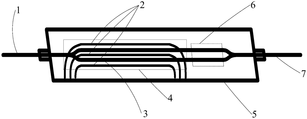
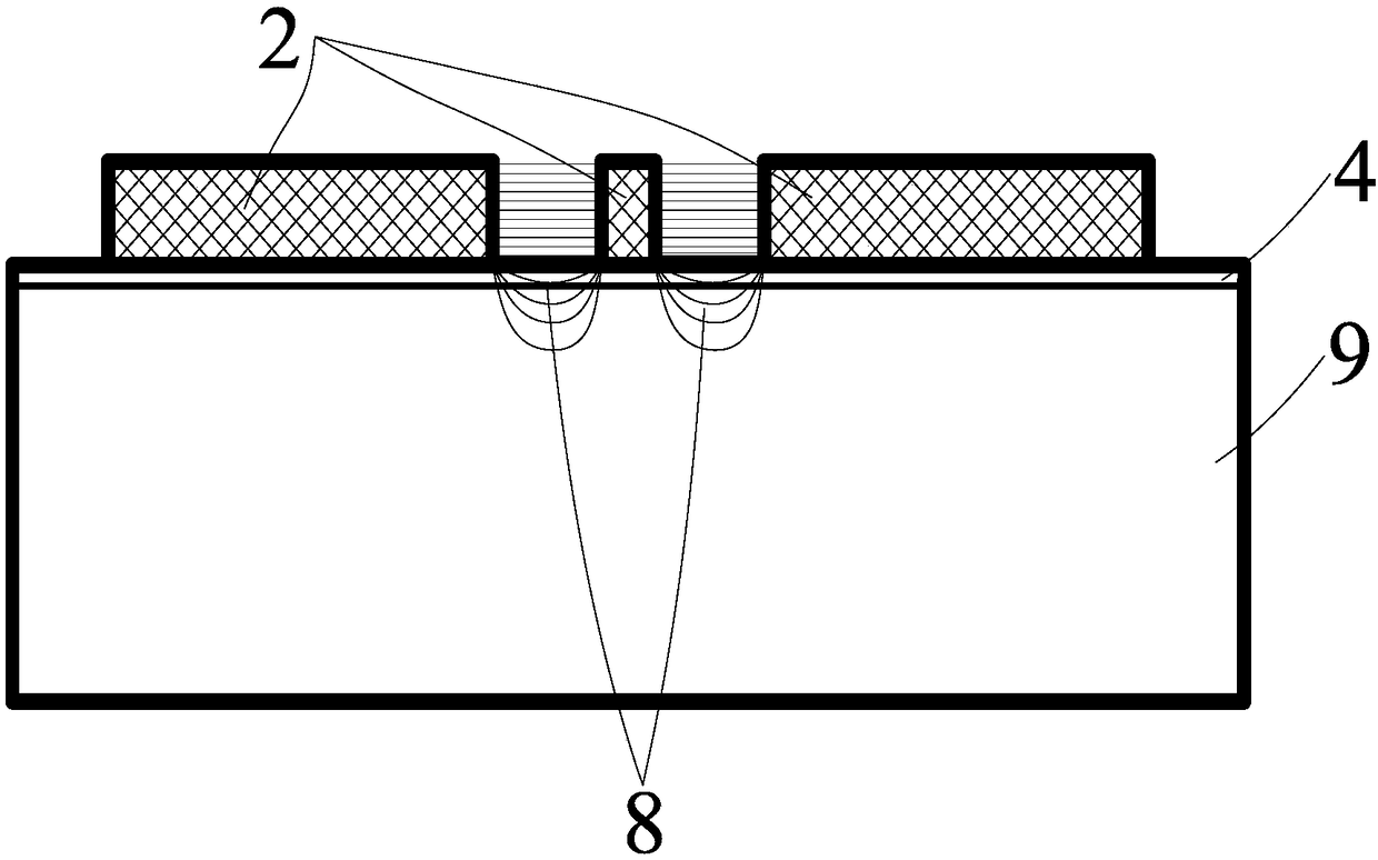
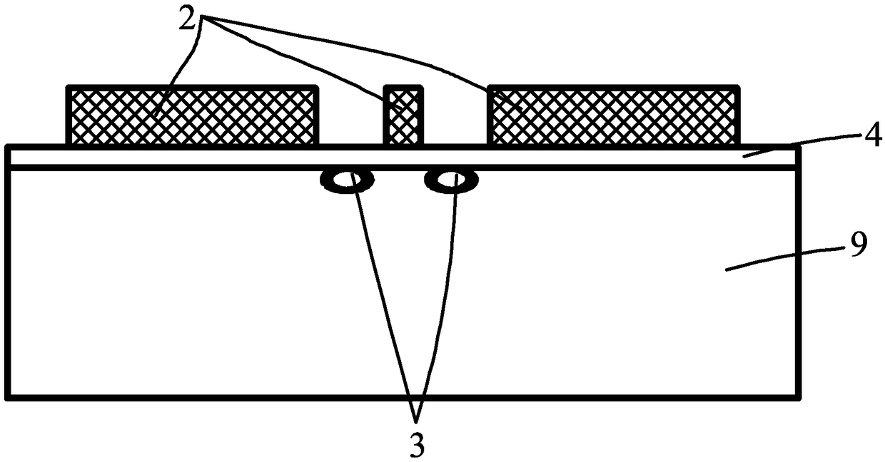
[0028] The present invention proposes a high-speed electro-optic modulator based on a lithium niobate thick film, including a supporting substrate 9, a bonding layer 11, an optical waveguide 3 and a modulation electrode 2, and the bonding layer 11 is located on the upper surface of the supporting substrate 9 , the optical waveguide 3 and the modulation electrode 2 are located on the surface of the bonding layer 11, and a layer of lithium niobate thick film 13 i...


PUM

PropertyMeasurementUnit
Thicknessaaaaaaaaaa
Thicknessaaaaaaaaaa

Abstract

The invention relates to the field of integrated optics, in particular to a lithium niobate thick film-based high-speed electro-optical modulator and a preparation method thereof; the modulator comprises a supporting substrate, a bonding layer, an optical waveguide and a modulation electrode, wherein the optical waveguide is located on the surface of the bonding layer, and a layer of lithium niobate thick film is arranged on the bonding layer; the thickness of the lithium niobate thick film is 8-20 microns; by virtue of about 10 microns of the ridge height of the thick-film lithium niobate, the modulation efficiency can be improved by 60% or above, and the substrate is only 8-20 microns in thickness due to the thinning technology, so that the resonance effect can be avoided, and the high-speed broadband can be further realized; and compared with a thin film type waveform lithium niobate modulator, the lithium niobate thick film-based high-speed electro-optical modulator has the advantages of being low in diffusion type optical waveguide transmission loss and low in coupling loss.

Description

technical field [0001] The invention relates to the field of integrated optics, in particular to a high-speed electro-optic modulator based on lithium niobate thick film and a preparation method thereof. Background technique [0002] The typical structure of a lithium niobate intensity modulator chip (taking an X-cut Y-passed lithium niobate chip as an example) is as follows: figure 1 As shown, the electric field distribution is as figure 2 shown. [0003] In order to reduce the half-wave voltage and achieve high-speed broadband. Researchers first used wet or dry etching to form a ridge-shaped lithium niobate optical waveguide structure to increase the overlap integral Γ of the electric field and the optical field. The height of the waveguide ridge is generally not more than 3 microns, and the etching process will also cause the side wall of the ridge optical waveguide to be rough, which will greatly increase the transmission loss of light. Therefore, the researchers com...

Claims


Application Information

Patent Timeline
IPC IPC(8): G02F1/03G02F1/035
CPCG02F1/0305G02F1/0316G02F1/035
Inventor 华勇舒平雷成龙曾健
Owner THE 44TH INST OF CHINA ELECTRONICS TECH GROUP CORP
Why Eureka
Try Eureka