Three-dimensional memory structure and manufacturing method thereof
A manufacturing method and memory technology, applied in the field of memory, can solve the problems of reducing storage density, large chip area, smaller core area, etc., and achieve the effect of reducing wiring density, saving area, and providing storage density
- Summary
- Abstract
- Description
- Claims
- Application Information
AI Technical Summary
Problems solved by technology
Method used
Image


Examples
Embodiment Construction
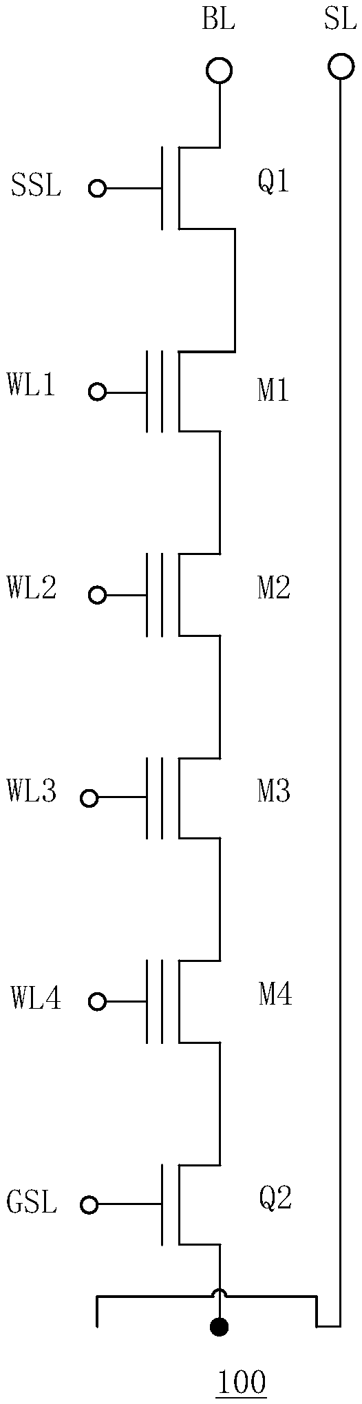
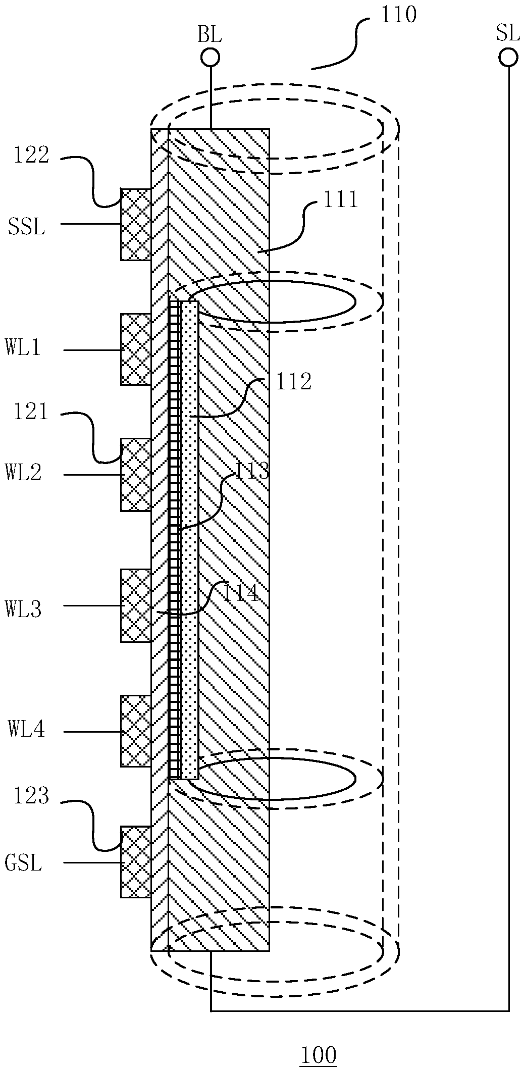
[0023] Various embodiments of the invention will be described in more detail below with reference to the accompanying drawings. In the various drawings, the same elements are denoted by the same or similar reference numerals. For the sake of clarity, various parts in the drawings have not been drawn to scale.
[0024] The specific implementation manners of the present invention will be further described in detail below in conjunction with the accompanying drawings and embodiments.
[0025] "Above" described in the present invention refers to being located above the plane of the substrate, which may refer to direct contact between materials, or may be arranged at intervals.
[0026] In the present application, the term "semiconductor structure" refers to a general designation of the entire semiconductor structure formed in various steps of manufacturing a memory device, including all layers or regions that have been formed. In the following, many specific details of the prese...
PUM
 Abstract
Description
Claims
Application Information
 - R&D
- Intellectual Property
- Life Sciences
- Materials
- Tech Scout
- Unparalleled Data Quality
- Higher Quality Content
- 60% Fewer Hallucinations
Browse by: Latest US Patents, China's latest patents, Technical Efficacy Thesaurus, Application Domain, Technology Topic, Popular Technical Reports.
© 2025 PatSnap. All rights reserved.Legal|Privacy policy|Modern Slavery Act Transparency Statement|Sitemap|About US| Contact US: help@patsnap.com