Packaging antenna and manufacturing method thereof

A manufacturing method and antenna technology, applied to antennas, antenna parts, antenna grounding devices, etc., can solve the problems of not providing process customization services, increasing application costs, increasing parasitic parameters, etc., and meeting the requirements of high-precision millimeter wave antennas and feeders Graphical requirements, reduced parasitic parameters, and high dimensional accuracy

Active Publication Date: 2019-02-12
TSINGHUA UNIV
View PDF3 Cites 7 Cited by
  • Summary
  • Abstract
  • Description
  • Claims
  • Application Information

AI Technical Summary

Problems solved by technology

For millimeter-wave chip AiP packaging, the traditional packaging technology is to fan out the MMIC chip and integrate it into the AiP system, but this will increase the parasitic parameters of the interconnection
[0008] In addition, many manufacturers currently provide fan-out packaging processes, such as Infineon's eWLB (embedded Wafer Level Ball gridarray, embedded wafer-level ball grid array packaging), TSMC's InFO-WLP, etc., but do not provide process Customized service
Taking the eWLB process as an example, the package structure manufactured by the eWLB process has only one RDL rewiring layer. When implementing AiP, if the RDL metal layer is used to form the antenna pattern, it is impossible to make a reflective ground plane on the eWLB package, and only a PCB can be used. (Printed Circuit Board, printed circuit board) The wiring layer on the ground plane needs to carefully optimize the PCB structure to cooperate with the antenna design, which brings trouble to the application and increases the application cost

Method used


Image

  • Packaging antenna and manufacturing method thereof
  • Packaging antenna and manufacturing method thereof
  • Packaging antenna and manufacturing method thereof

Examples


Embodiment Construction

[0047] Specific embodiments of the present disclosure will be described in detail below in conjunction with the accompanying drawings. It should be understood that the specific embodiments described here are only used to illustrate and explain the present disclosure, and are not intended to limit the present disclosure.

[0048] In this disclosure, unless stated otherwise, the used orientation words such as "upper and lower" generally refer to upper and lower in the corresponding drawings, and "inner and outer" refer to the inner part relative to the outline of the part itself. ,outside. In addition, the used terms such as "first" and "second" are only used to distinguish one element from another element, and do not have sequence or importance.

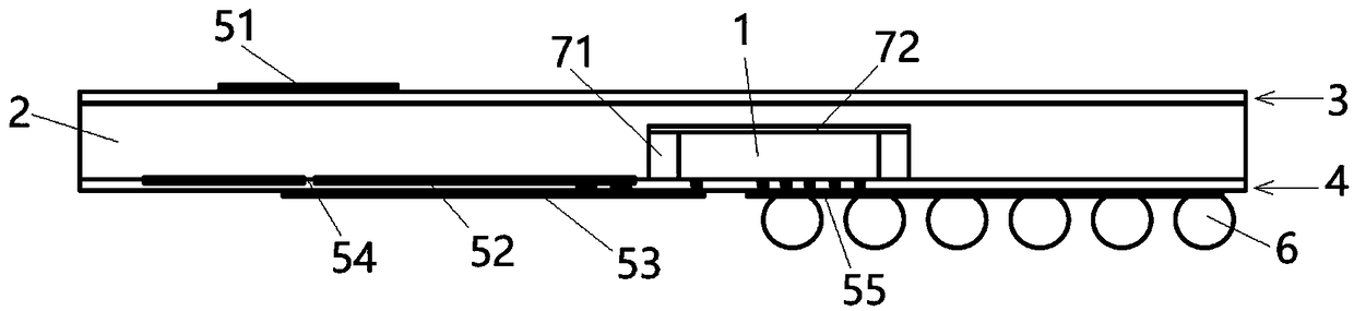
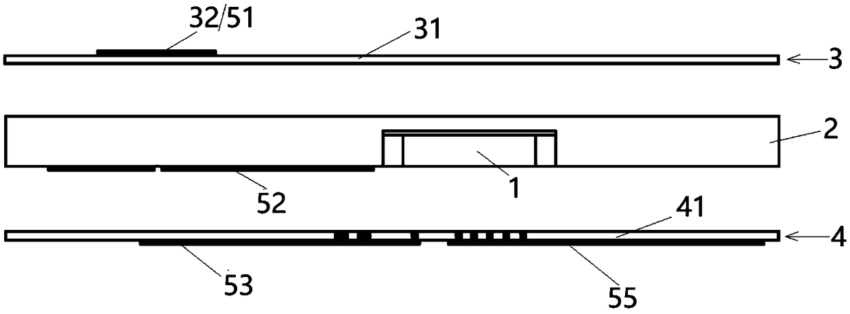
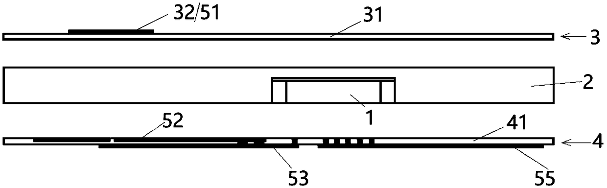
[0049] In the field of antenna-on-package technology, since the accuracy of the radiation patch affects the resonant frequency, and the accuracy of the feeder affects the characteristic impedance and matching, millimeter-wave antenna...


PUM


Abstract

The invention relates to packaging antenna and a manufacturing method thereof. The packaging antenna comprises a chip, a substrate, a first rewiring layer and a second rewiring layer, wherein the chipis fixed in the substrate; one surface of the substrate presses the first rewiring layer, the other surface of the substrate presses the second rewiring layer, wherein the first rewiring layer manufactures an antenna pattern, the second rewiring layer manufactures a reflecting ground plane and a feeder pattern, ore the reflecting ground plane is formed by a substrate metal layer. By the packagingantenna, the parasitic parameter of the packaging antenna is reduced, and meanwhile, the performance of the antenna is improved.

Description

technical field [0001] The present disclosure relates to the technical field of packaged antennas, and in particular, to a packaged antenna and a method for manufacturing the packaged antenna. Background technique [0002] With the development of science and technology in recent decades, millimeter waves have gradually developed towards civilian miniaturization and multi-function, and have been widely used in automotive radar, high-speed data communication, industrial automation sensors, and medical equipment. Antenna is an important part in a wireless system, there are two forms of separation and integration. The integrated antenna includes two types: Antenna-on-Chip ("AoC" for short) and Antenna-in-Package ("AiP" for short). The antenna-on-chip technology integrates the antenna and other circuits on the same chip through semiconductor materials and processes. The advantages are high integration, no additional interconnection, and small parasitic effects, especially for th...

Claims


Application Information

Patent Timeline
Patent Type & Authority Applications(China)
IPC IPC(8): H01L23/66H01L23/498H01L23/52H01L21/48H01L21/768H01Q1/22H01Q1/38H01Q1/48H01Q1/50H01Q19/10
CPCH01L23/49816H01L23/49838H01L23/52H01L23/66H01Q1/2283H01Q1/38H01Q1/48H01Q1/50H01Q19/104H01L21/4846H01L21/4853H01L21/76895H01L2224/73267H01L2224/04105H01L2224/12105H01L2924/15153H01L2224/32225H01L2223/6677
Inventor 王谦蔡坚张雪松周晟娟
Owner TSINGHUA UNIV
Why Eureka
Try Eureka