Array substrate, preparation method of array substrate, and display panel

An array substrate and quantum dot light-emitting technology, which is applied in semiconductor/solid-state device manufacturing, electrical components, electric solid-state devices, etc., can solve problems such as climbing the quantum dot light-emitting layer, increasing the limit of mass production of QLED display panels, etc.

Inactive Publication Date: 2019-02-15
BOE TECH GRP CO LTD +1
View PDF3 Cites 10 Cited by
  • Summary
  • Abstract
  • Description
  • Claims
  • Application Information

AI Technical Summary

Problems solved by technology

To prepare a high-resolution QLED display panel, the interval between adjacent sub-pixels is small, and the size of the pixel-defining layer in the pixel-defining area is also small, which is more likely to cause the quantum dot light-emitting layer to climb

Method used


Image

  • Array substrate, preparation method of array substrate, and display panel
  • Array substrate, preparation method of array substrate, and display panel
  • Array substrate, preparation method of array substrate, and display panel

Examples


Embodiment Construction

[0037] The following will clearly and completely describe the technical solutions in the embodiments of the present invention with reference to the accompanying drawings in the embodiments of the present invention. Obviously, the described embodiments are only some, not all, embodiments of the present invention. Based on the embodiments of the present invention, all other embodiments obtained by persons of ordinary skill in the art without making creative efforts belong to the protection scope of the present invention.

[0038] An embodiment of the present invention provides a method for preparing an array substrate, such as figure 1 As shown, it can be realized through the following steps:

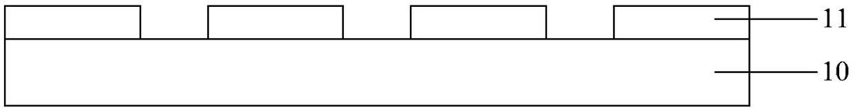
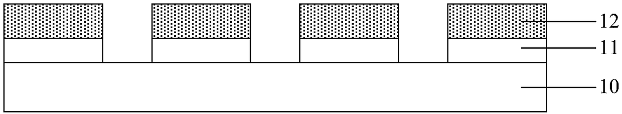
[0039] S11, such as figure 2 As shown, a first electrode 11 is formed in each sub-pixel region on the substrate 10 .

[0040] Here, when the first electrode 11 is an anode, the material of the first electrode 11 may be, for example, indium tin oxide (Indiumtin oxide, ITO for short); or...


PUM


Abstract

Embodiments of the invention provide an array substrate, a preparation method of the array substrate and a display panel, relate to the technical field of display, and a quantum dot light-emitting layer can be prevented from climbing on a pixel definition layer, so that the thickness uniformity of the quantum dot light-emitting layer is avoided. The preparation method of the array substrate comprises the steps that a first electrode is formed in each sub-pixel area on a substrate; a quantum dot light-emitting layer is formed in each sub-pixel area and above the first electrode; a pixel definition layer is formed on a substrate where the first electrode and the quantum dot light-emitting layer are formed, wherein the pixel definition layer is located between any adjacent quantum dot light-emitting layers; and in each sub-pixel area, a second electrode is formed above the quantum dot light-emitting layer.

Description

technical field [0001] The present invention relates to the field of display technology, in particular to an array substrate, a preparation method thereof, and a display panel. Background technique [0002] With the rapid development of organic materials and quantum dot materials, organic electroluminescent devices (Organic Light-Emitting Diode, referred to as OLED) and quantum dot electroluminescent devices (Quantum Dot Light Emitting Diodes, referred to as QLED) are also progressing rapidly. Moreover, with the improvement of consumer consumption level, high-resolution products have become the key development direction of display products. [0003] Due to its potential advantages in wide color gamut and high lifespan, QLED has attracted more and more attention. Its research has deepened, its quantum efficiency has continued to improve, and it has basically reached the level of industrialization. Realizing its industrialization has become the trend of the future. [0004] ...

Claims


Application Information

Patent Timeline
IPC IPC(8): H01L27/32H01L51/50
CPCH10K59/121H10K59/122H10K59/12H10K50/115H01L33/06H01L27/156H10K50/16H10K50/171H10K71/00H10K59/1201
Inventor 李东
Owner BOE TECH GRP CO LTD
Why Eureka
Try Eureka