Display panel, display device and display panel manufacturing method

A technology for a display panel and a manufacturing method, which is applied in the manufacturing of semiconductor/solid-state devices, instruments, semiconductor devices, etc., can solve the problems of reducing the light transmittance of the display panel, high cost, strict glass cutting accuracy and process capability, etc.

Active Publication Date: 2019-02-22
XIAMEN TIANMA MICRO ELECTRONICS
View PDF6 Cites 22 Cited by
  • Summary
  • Abstract
  • Description
  • Claims
  • Application Information

AI Technical Summary

Problems solved by technology

Placing the camera with an opening in the display area of ​​the display can maximize the screen-to-body ratio, but the hole-digging technology requires very strict glass cutting accuracy and process capabilities, so this method faces problems such as low production capacity, low yield, and h

Method used


Image

  • Display panel, display device and display panel manufacturing method
  • Display panel, display device and display panel manufacturing method
  • Display panel, display device and display panel manufacturing method

Examples


Embodiment Construction

[0037] The present invention will be further described in detail below in conjunction with the accompanying drawings and embodiments. It should be understood that the specific embodiments described here are only used to explain the present invention, but not to limit the present invention. In addition, it should be noted that, for the convenience of description, only some structures related to the present invention are shown in the drawings but not all structures.

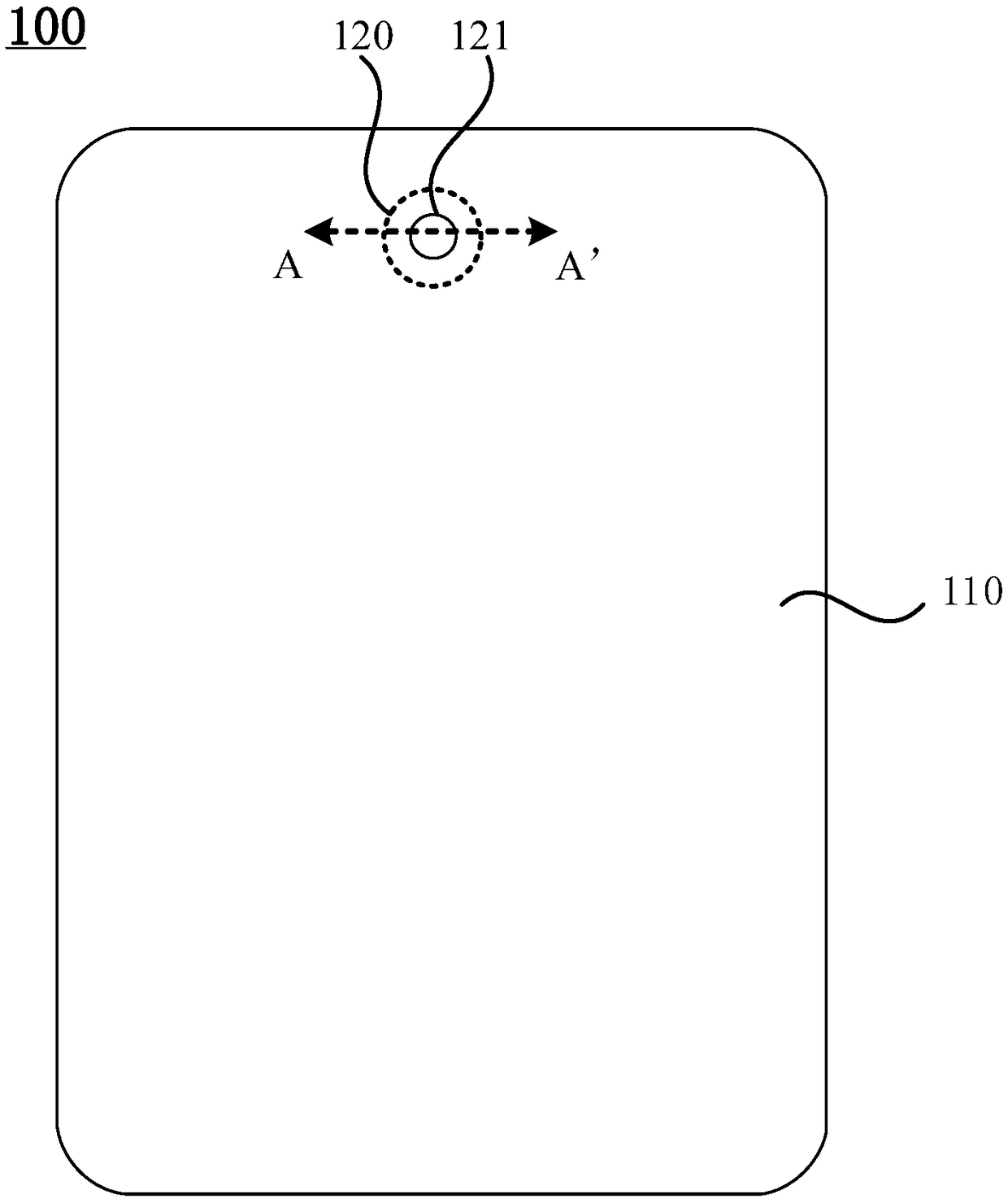
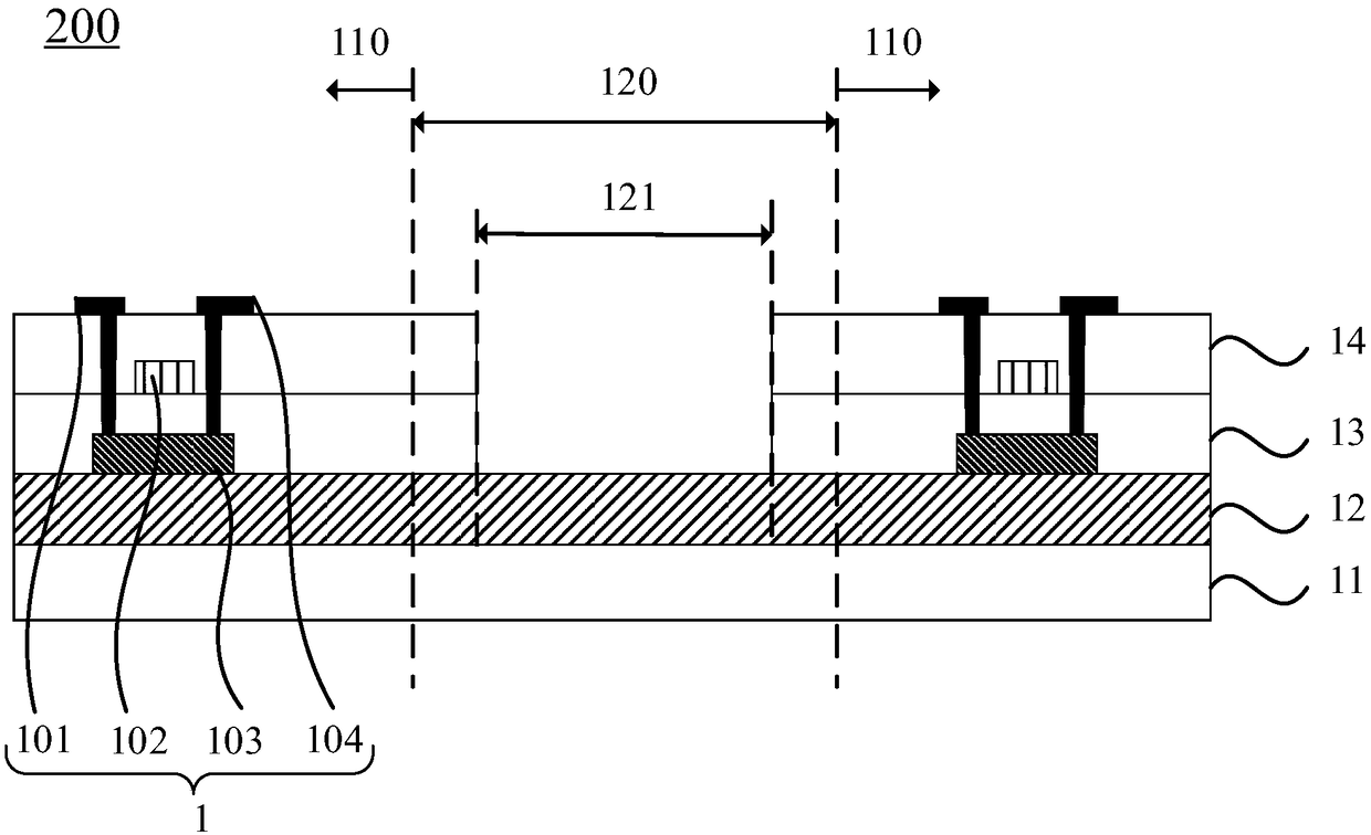
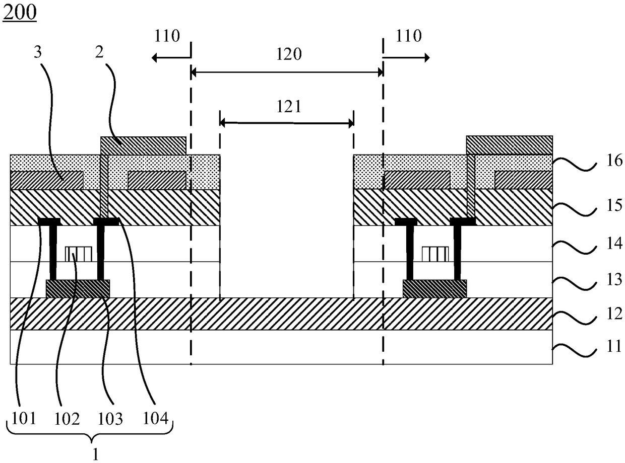
[0038] figure 1 It is a schematic top view structural diagram of a display panel provided by an embodiment of the present invention, figure 2 for along figure 1 Schematic diagram of the cross-sectional structure in the direction of AA', refer to figure 1 with figure 2 , the display panel 100 includes a display area 110 and a non-display area 120, the display area 110 surrounds the non-display area 120, the non-display area 120 includes a module setting area 121, and the light transmittance of the display pane...


PUM


Abstract

The present invention provides a display panel, a display device, and a display panel manufacturing method. The display panel includes a display area and a non-display area; the display area surroundsthe non-display area; the non-display area includes a module setting area; the light transmittance of the display panel in the module setting area is greater than a preset value; the display panel includes an array substrate; the array substrate includes: a first substrate; a buffer layer located at one side of the first substrate; a plurality of thin film transistors located on a side of the buffer layer away from the first substrate; a film layer where the plurality of thin film transistors are located only exists in a region of the non-display area except the module setting area and the display area; and the buffer layer is present in the display area and the non-display area, and covers the module setting area. The invention aims to improve the light transmittance of the display panelin the module setting area, reduce the process and improve the production efficiency.

Description

technical field [0001] The present invention relates to the field of display technology, in particular to a display panel, a display device and a method for manufacturing the display panel. Background technique [0002] With the continuous development of display technology, display screens such as "borderless" and "full screen" have become research hotspots in the display field. A larger screen-to-body ratio brings users a better visual experience and can display more information. Therefore, pursuing a larger screen-to-body ratio has become the mainstream development trend of display products. [0003] In the existing technology, in order to pursue a high screen-to-body ratio, the display products continue to compress the frame, and at the same time design a special-shaped screen. The full screen with a hole structure will become the latest design trend. The hole position can be used to place devices such as cameras and earpieces. Placing the camera with an opening in the d...

Claims


Application Information

Patent Timeline
IPC IPC(8): H01L27/12H01L21/84
CPCH01L27/1218H01L27/1262G02F1/1333G02F1/1362G02F1/1368G02F1/133512G02F1/13394H10K50/8428
Inventor 杨雁郑斌义吴玲沈柏平
Owner XIAMEN TIANMA MICRO ELECTRONICS
Why Eureka
Try Eureka