Inductance testing device and method for wave-absorbing material

A technology of wave absorbing material and testing device, which is applied in the direction of measuring device, measuring electrical variable, measuring resistance/reactance/impedance, etc., and can solve problems such as poor performance, high brittleness, and damage.

Pending Publication Date: 2019-03-01
SHANGHAI LINEPRINTING MATERIALS CO LTD
View PDF0 Cites 4 Cited by
  • Summary
  • Abstract
  • Description
  • Claims
  • Application Information

AI Technical Summary

Problems solved by technology

However, the surface of the coated wave absorbing material is rough, brittle, too thick, and its performance is poor, so it cannot be directly used in the field of radiation protection. It needs to go through a series of production processes to change the appearance and performance of the ferrite wave absorbing material. In order to meet the quality requirements of customers, the product performance needs to be monitored during the processing process. The traditional monitoring method is to measure the destructive magnetic permeability of the absorbing material to achieve quality monitoring. Because the destructive test is only for the product during the production process Sampling inspection, due to the fluctuation of process factors, the product quality will be unstable. At this time, 100% quality monitoring cannot be carried out, resulting in the flow of defective products to the client, and finally to consumers. Therefore, how to achieve 100% quality without destroying the product Monitoring has great practical significance for quality monitoring in the production process

Method used


Image

  • Inductance testing device and method for wave-absorbing material
  • Inductance testing device and method for wave-absorbing material
  • Inductance testing device and method for wave-absorbing material

Examples


Embodiment 1

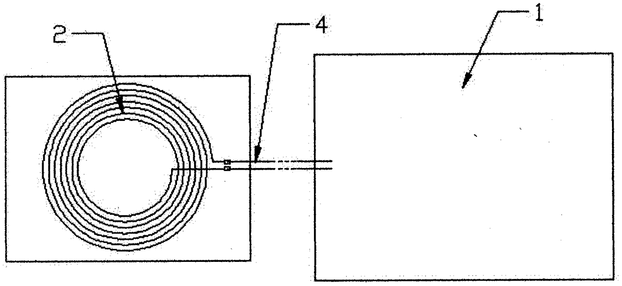
[0028] Such as Figure 1-4 As shown, the inductance testing device of a kind of wave-absorbing material of the present invention is used for detecting the inductance value of its wave-absorbing material, and this device comprises LCR test instrument 1, coil 2 and test jig; The model of described LCR test instrument 1 is Taiwan Goodwill LCR-8110G, the structure and working principle of the LCR testing instrument 1 are prior art, and will not be repeated here; the LCR testing instrument 1 and the coil 2 are connected by a metal wire 4; the coil 2 set in the test fixture;

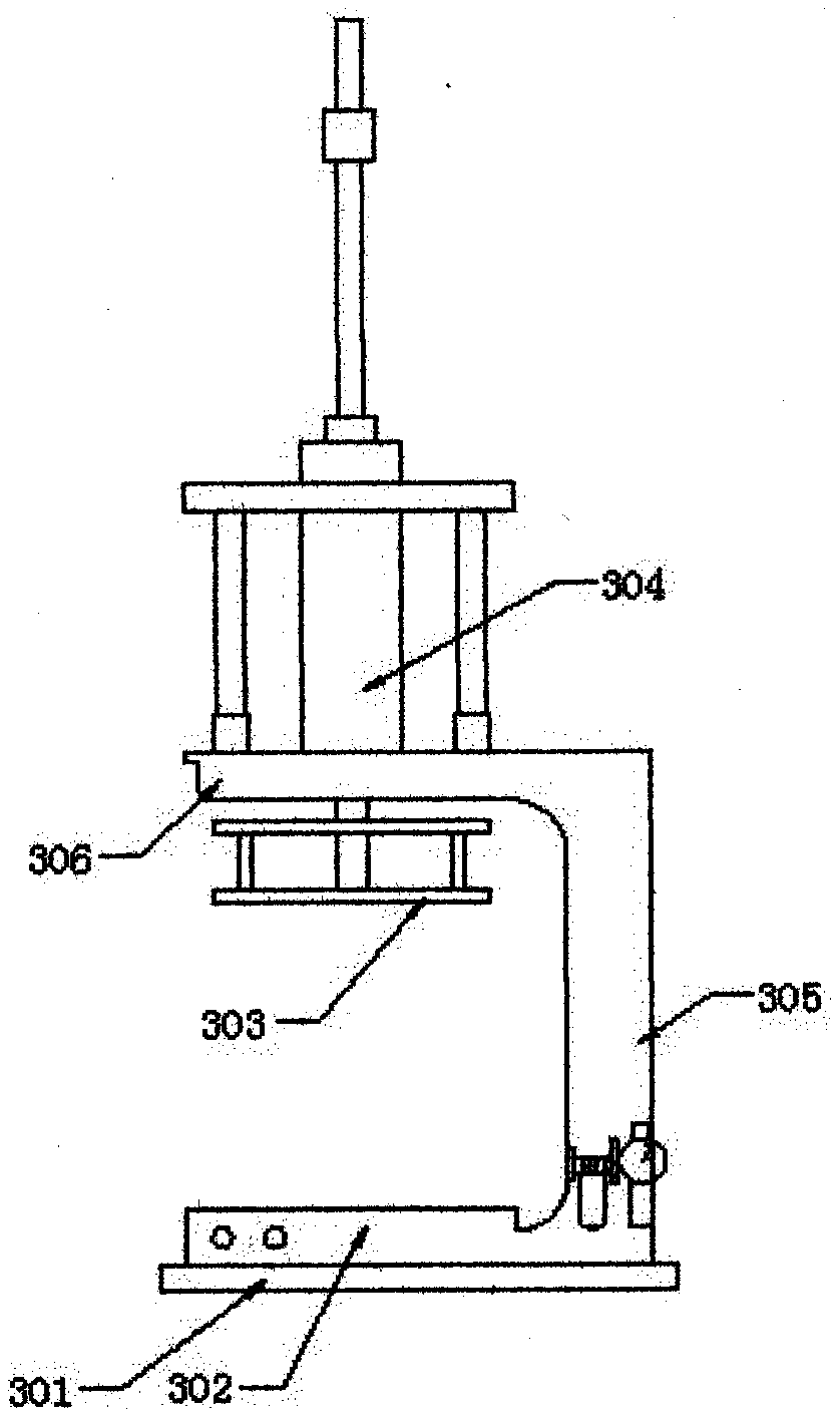
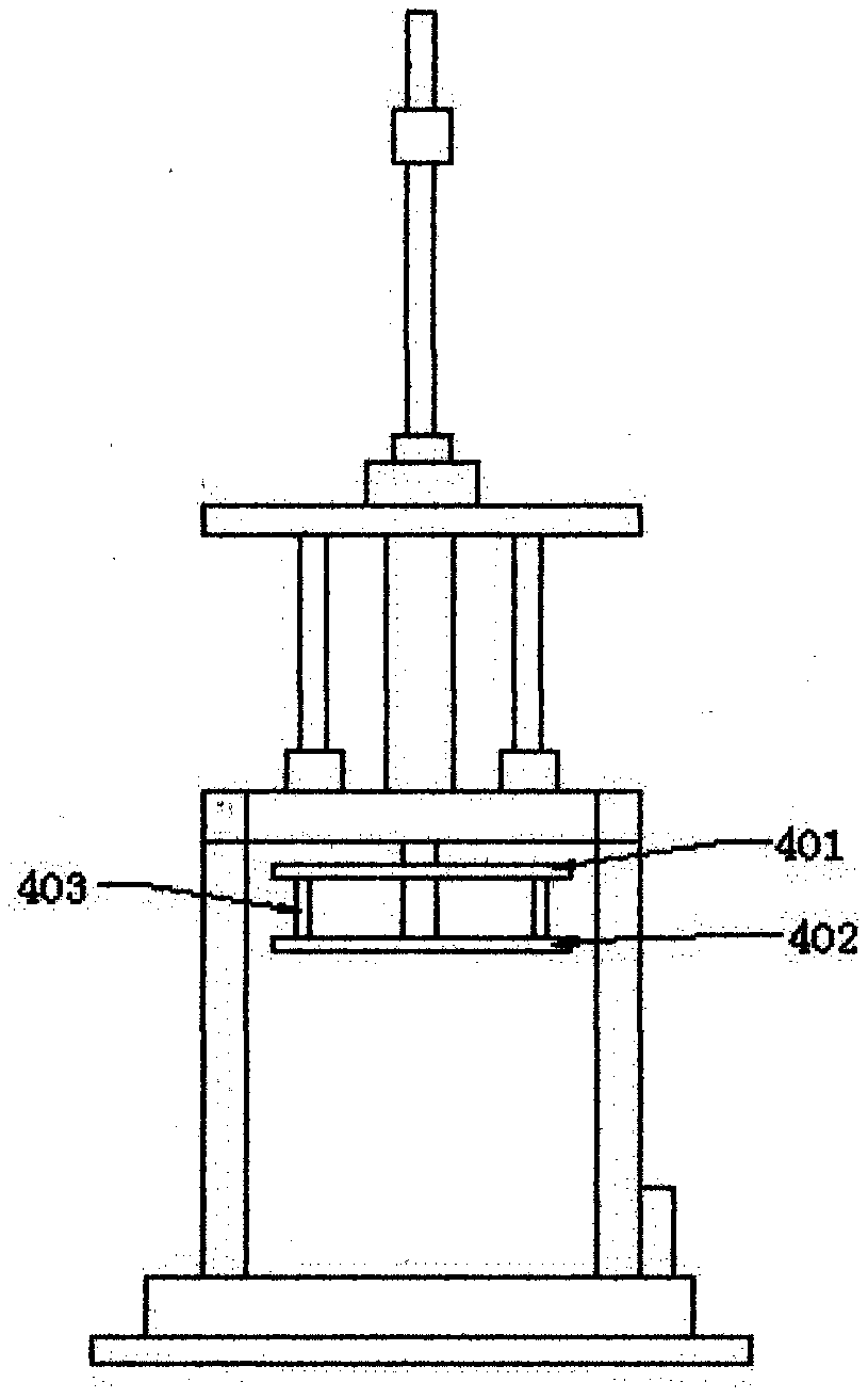
[0029] The test fixture includes a base 301, a lower table 302, an upper platen 303, a lower pressure cylinder 304, a column 305, a top plate 306, a groove 307 and a film 308; the lower table 302 is fixed above the base 301 The base 301 is provided with a fixed bracket behind the lower table surface 302; the fixed bracket includes a column 305 fixedly arranged on the rear end of the base 301 and a top plate 3...

Embodiment 2

[0035] A method for testing the inductance of a wave-absorbing material, comprising the steps of:

[0036] Step 1: Turn on the main power switch of the LCR tester 1, turn on the air pressure switch, set the applied pressure and pressing time, the applied pressure range is 2-5kg / cm2, and the pressing time is 2-5s;

[0037] Step 2: Coil 2 installation: Select a coil 2 with a line width of 1.0-2.0mm, a line spacing of 0.1-0.2mm, a number of turns of 10-20 turns, and a thickness of 1.0-2.0o / z to pass the metal wire 4 and LCR test The instrument 1 is connected, the coil 2 is connected and fixed in the groove 307 of the lower table 302 on the test fixture, and the LCR test instrument 1 is opened;

[0038] Step 3: Put a film 308 with a thickness of 0.10-0.50mm on the lower table 302 of the test fixture, and confirm the inductance Ls value, which is stable at 7.951uh and normal;

[0039] Step 4: Place a piece of microwave-absorbing material of known thickness on the lower table 302 o...


PUM


Abstract

The invention discloses an inductance testing device and method for a wave-absorbing material, and the device comprises an LCR testing instrument, a coil and a test jig. The LCR testing instrument andthe coil are connected by a metal wire. The test jig has upper and lower layers. In other words, the lower table is fixed, the middle part is provided with a groove which enables the coil to be fixedin the groove, and a film is placed on the lower table surface. A lower pressure cylinder drives an upper pressure plate to move up and down and generates a certain pressure, so as to achieve close contact with the upper and lower parts, and then the LCR testing instrument is connected with the coil through the metal wire, so as to measure the inductance value of the wave-absorbing material, anddetermines whether the inductance of the wave-absorbing material is qualified or not through the reference of the "Inductance Value and Thickness Standard Correspondence Table", so as to detect the performance of a product. The device of the invention can achieve the measurement of different points of a single film or measurement of the single film for many times, and achieves 100% quality monitoring on the basis that the wave-absorbing material is not damaged, and enables processed wave-absorbing material to meet the requirements of a customer for the quality.

Description

technical field [0001] The invention relates to an inductance testing device and a testing method of a wave-absorbing material, belonging to the technical field of wave-absorbing material testing. Background technique [0002] Controlling electromagnetic pollution and developing and preparing a material that can resist and weaken electromagnetic radiation—absorbing materials—is a major direction of today's material manufacturing industry. [0003] Common coated wave-absorbing materials are composed of binders and absorbents, which are simple and practical to manufacture. However, the surface of the coated wave absorbing material is rough, brittle, too thick, and its performance is poor, so it cannot be directly used in the field of radiation protection. It needs to go through a series of production processes to change the appearance and performance of the ferrite wave absorbing material. In order to meet the quality requirements of customers, the product performance needs t...

Claims


Application Information

Patent Timeline
Patent Type & Authority Applications(China)
IPC IPC(8): G01R27/26
CPCG01R27/26
Inventor 朱世民韦杰
Owner SHANGHAI LINEPRINTING MATERIALS CO LTD
Why Eureka
Try Eureka