A thin film preparation process and a gas sensor preparation method related to the process

A gas sensor and organic semiconductor technology, applied in the field of gas sensor preparation and thin film preparation technology, can solve problems such as erosion and uneven thickness of thin films, achieve thin film flattening, reduce hysteresis effect, and enhance the effect of interaction

Active Publication Date: 2020-10-09
UNIV OF ELECTRONICS SCI & TECH OF CHINA
View PDF2 Cites 0 Cited by
  • Summary
  • Abstract
  • Description
  • Claims
  • Application Information

AI Technical Summary

Problems solved by technology

[0006] The invention provides a film preparation process and a gas sensor preparation method related to the process to solve the technical problems of solvent erosion of the lower film and uneven film thickness in the existing film preparation process

Method used


Image

  • A thin film preparation process and a gas sensor preparation method related to the process
  • A thin film preparation process and a gas sensor preparation method related to the process
  • A thin film preparation process and a gas sensor preparation method related to the process

Examples


Embodiment 1

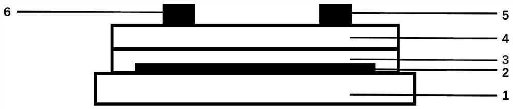
[0033] Such as figure 1 Shown is a field effect transistor gas sensor with a bottom-gate top-contact structure. The material and thickness of each layer are: the gate electrode 2, the source electrode 5, and the drain electrode 6 are all silver nanowires, and the dielectric layer 3 is made of polystyrene. The thickness is 500nm, and the semiconductor layer 4 is Tips-pentacene with a thickness of 30nm. The preparation process of the gas sensor is as follows:

[0034] ① Clean the substrate 1 with detergent, acetone solution, deionized water and isopropanol solution, and dry it with nitrogen after cleaning;

[0035] ②Preparing a silver nanowire grid electrode 2 on the surface of the substrate 1;

[0036] ③ preparing a polystyrene dielectric layer 3 on the gate electrode 2;

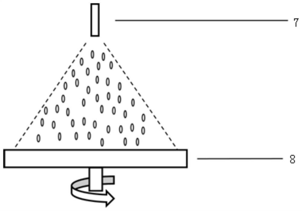
[0037] ④The Tips-pentacene solution is sprayed vertically from top to bottom at a speed of 40uL / s onto the dielectric layer 3 rotating at 3000rad / min to prepare a semiconductor layer 4 (the preparation pro...

Embodiment 2

[0040] On the basis of Example 1, the dielectric layer 3 is changed to polymethyl methacrylate with a thickness of 400 nm; the semiconductor layer 4 is Tips-pentacene with a thickness of 30 nm. The preparation process of the gas sensor is as follows:

[0041] ① Clean the substrate 1 with detergent, acetone solution, deionized water and isopropanol solution, and dry it with nitrogen after cleaning;

[0042] ②Preparing a silver nanowire grid electrode 2 on the surface of the substrate 1;

[0043] ③ preparing a polymethyl methacrylate dielectric layer 3 on the gate electrode 2;

[0044] ④The Tips-pentacene solution is sprayed vertically from top to bottom at a speed of 60uL / s onto the dielectric layer 3 rotating at 3000rad / min to prepare a semiconductor layer 4 (the preparation process is as follows: figure 2 shown);

[0045] ⑤ Prepare the silver nanowire source electrode 5 and the drain electrode 6 on the organic semiconductor layer 4, that is, make a field effect transistor...

Embodiment 3

[0047] On the basis of Example 1, the dielectric layer 3 is changed to polystyrene with a thickness of 500 nm, and the semiconductor layer is Tips-pentacene with a thickness of 30 nm. The preparation process of the gas sensor is as follows:

[0048] ① Clean the substrate 1 with detergent, acetone solution, deionized water and isopropanol solution, and dry it with nitrogen after cleaning;

[0049] ②Preparing a silver nanowire grid electrode 2 on the surface of the substrate 1;

[0050] ③ preparing a polystyrene dielectric layer 3 on the gate electrode 2;

[0051] ④The Tips-pentacene solution is vertically sprayed from top to bottom at a speed of 80uL / s onto the dielectric layer 3 rotating at 3000rad / min to prepare a semiconductor layer 4 (the preparation process is as follows: figure 2 shown);

[0052]⑤ Prepare the silver nanowire source electrode 5 and the drain electrode 6 on the organic semiconductor layer 4, that is, make a field effect transistor gas sensor.


PUM

PropertyMeasurementUnit
thicknessaaaaaaaaaa
thicknessaaaaaaaaaa
thicknessaaaaaaaaaa

Abstract

The invention discloses a film preparation process and a gas sensor preparation method related to the process, and relates to the technical field of sensor preparation. The thin film preparation process adopted in the present invention integrates spin coating-spray coating process. After combining the traditional spin coating process and spray coating process, it has the advantages of uniform film formation by spin coating process and morphology regulation and control by spraying process. At the same time, the uniformity of the film is guaranteed. The atomized solution droplets are immediately spin-coated as soon as they touch the substrate, which solves the erosion of the upper layer solvent on the lower layer film during the solution method film preparation process, and forms a film with better uniformity. The independent spin-coating of droplets makes the organic semiconductor layer produce more grain boundaries, which effectively enhances the interaction between the gas to be measured and the organic semiconductor, and realizes the high-sensitivity detection of the gas to be measured by the device. At the same time, more grain boundaries are conducive to the diffusion of the gas. The recovery characteristics of the device are improved.

Description

technical field [0001] The invention relates to the technical field of sensor preparation, in particular to a film preparation process and a gas sensor preparation method related to the process. Background technique [0002] In the process of human production and life, a large amount of toxic and harmful gases are inevitably discharged into the atmosphere (for example: nitrogen dioxide, sulfur dioxide, ammonia, etc.). These harmful gases will not only destroy the ecological environment, but also seriously threaten people's health. Therefore, it is very important to realize the effective monitoring of the atmospheric environment. Among them, organic transistor gas sensors have the advantages of low consumption, room temperature operation, high sensitivity, multi-parameter detection and simple process compared with other traditional gas sensors. , simple preparation method, many types, and properties can be adjusted by molecular design, etc., have always attracted people's a...

Claims


Application Information

Patent Timeline
Patent Type & Authority Patents(China)
IPC IPC(8): H01L51/40H01L51/05G01N27/414
CPCG01N27/414H10K71/12H10K10/466
Inventor 于军胜侯思辉庄昕明王啸林
Owner UNIV OF ELECTRONICS SCI & TECH OF CHINA
Why Eureka
Try Eureka