

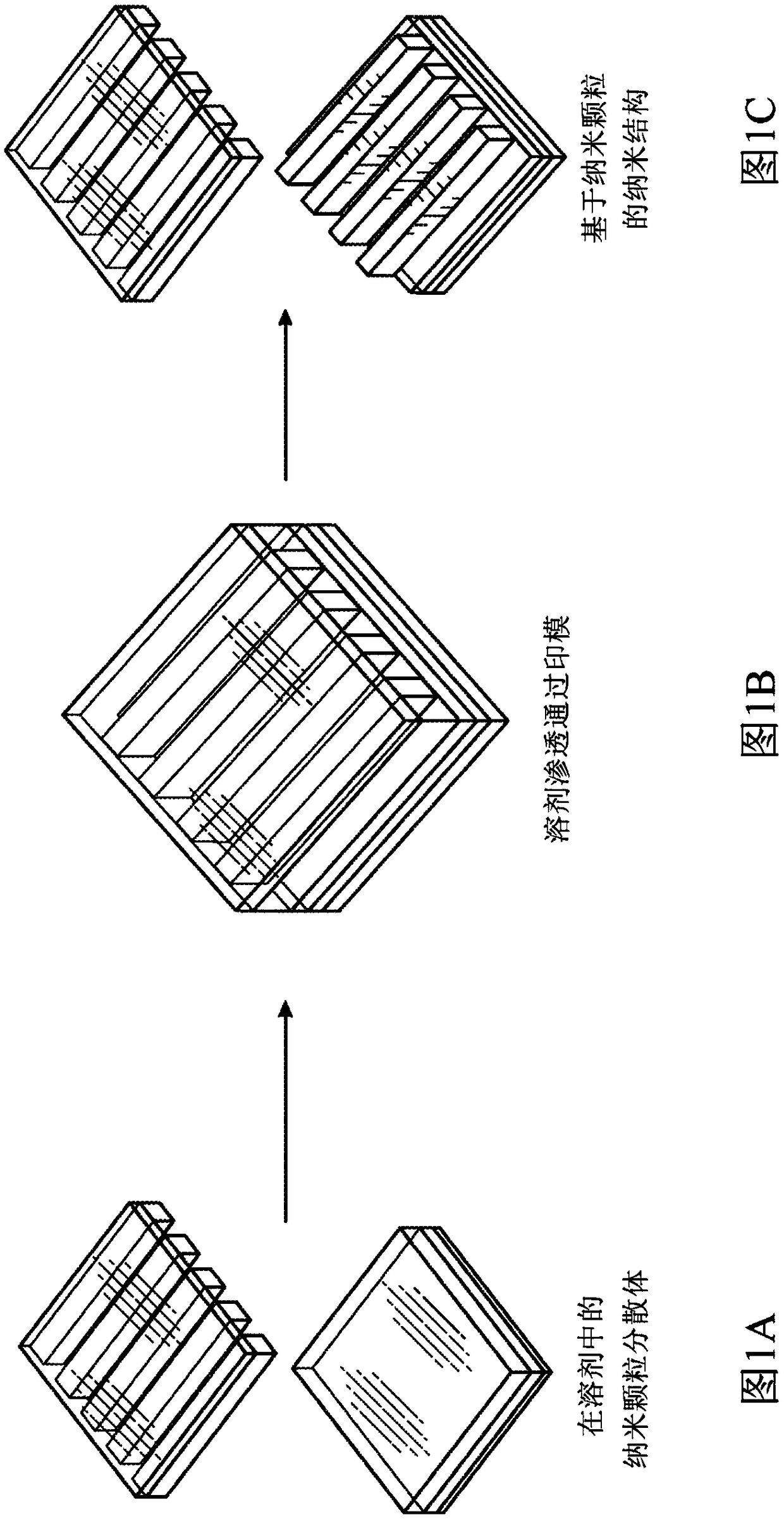
Patterning of nanostructures using imprint lithography
A technology of dimensional structure and nano-particles, which is applied in the direction of originals, applications, printing, etc. for photomechanical processing, and can solve problems such as shrinkage, feature deformation, and elevated temperature
- Summary
- Abstract
- Description
- Claims
- Application Information
AI Technical Summary
Problems solved by technology
Method used
Image

Examples
Embodiment Construction
[0084] Various embodiments of the present invention may be better understood by reference to the following examples, which are provided by way of illustration. The invention is not limited to the examples given herein.
[0085] Fabrication of PDMS impressions.
[0086] Patterned PDMS stamps were fabricated by casting PDMS on a silicon master. The silicon master was cleaned in concentrated sulfuric acid and then treated in an oxygen plasma cleaner for 15 minutes. The silicon master was then placed in a degassed glass jar at 80 °C, into which 1 volume percent of heptadecafluoro-1,1,2,2-tetrahydrodecyl)chlorosilane (Gelest Corp. ) for a period of 12 hours. During this process, self-assembled monolayers of long-chain fluorinated alkanes are produced on the silicon master, which lowers the surface energy of the silicon master and facilitates easy removal of the cured resin cast on it in the next step. PDMS impression.
[0087] PDMS stamps were prepared from silicon masters w...
PUM
| Property | Measurement | Unit |
|---|---|---|
| distance | aaaaa | aaaaa |
| height | aaaaa | aaaaa |
| wavelength | aaaaa | aaaaa |
Abstract
Description
Claims
Application Information