Array substrate and display device

A technology for array substrates and display devices, applied in static indicators, instruments, nonlinear optics, etc., can solve the problems of GOA circuit occupation, multiple wiring spaces, etc., and achieve the effect of realizing narrow frame, reducing coupling noise, and improving capacitance value

Active Publication Date: 2019-03-05
BOE TECH GRP CO LTD +1
View PDF6 Cites 9 Cited by
  • Summary
  • Abstract
  • Description
  • Claims
  • Application Information

AI Technical Summary

Problems solved by technology

[0007] Embodiments of the present invention provide an array substrate and a display device, which can solve the p

Method used


Image

  • Array substrate and display device
  • Array substrate and display device
  • Array substrate and display device

Examples


Embodiment Construction

[0034] The following will clearly and completely describe the technical solutions in the embodiments of the present invention with reference to the accompanying drawings in the embodiments of the present invention. Obviously, the described embodiments are only some, not all, embodiments of the present invention. Based on the embodiments of the present invention, all other embodiments obtained by persons of ordinary skill in the art without making creative efforts belong to the protection scope of the present invention.

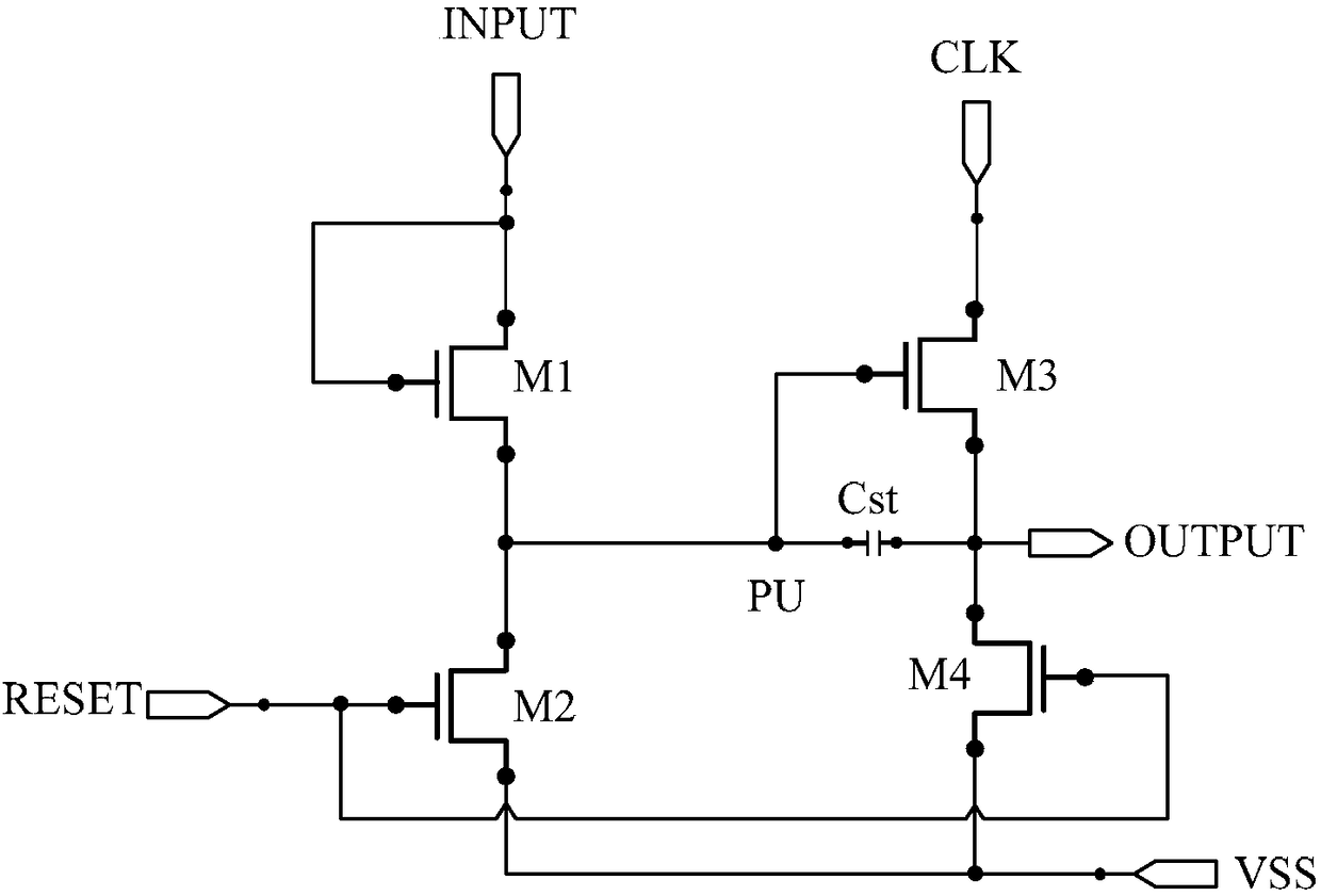
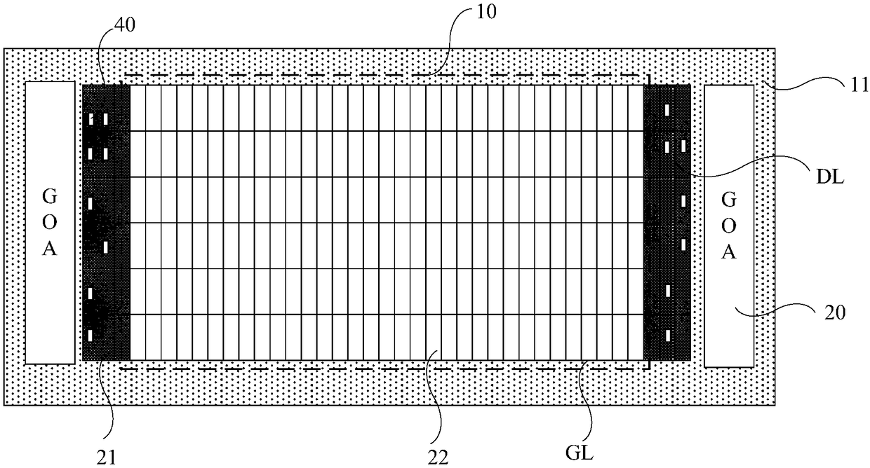
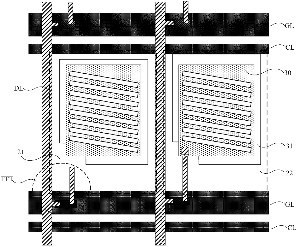
[0035] An embodiment of the present invention provides an array substrate, such as figure 2As shown, it includes an active display area 10 and a non-display area 11 located around the active display area 10 (Active Area, AA).

[0036] It should be noted that, the above-mentioned effective display area 10 is provided with gate lines GL (Gate Line) and data lines DL (Data Line) which intersect horizontally and vertically. The gate lines and the data lines DL i...


PUM


Abstract

Embodiments of the invention provide an array substrate and a display device, which belong to the technical field of displaying and can solve the problem that a GOA circuit occupies more wiring spacein order to increase the capacity of a bootstrap capacitor. The array substrate includes an effective display area and a non-display area located around the effective display area. The array substratefurther includes gate drive circuits and multiple rows of dummy sub-pixels located in the non-display area, and the dummy sub-pixels are disposed adjacent to the effective display area. Auxiliary capacitors are disposed in at least a portion of the dummy sub-pixels. Shift register units in the gate drive circuits are connected to the auxiliary capacitors, and the auxiliary capacitor at least constitutes a portion of bootstrap capacitors in the shift register units. The array substrate is used for forming the display device.

Description

technical field [0001] The present invention relates to the field of display technology, in particular to an array substrate and a display device. Background technique [0002] A display, such as a display panel of a TFT-LCD (Thin Film Transistor Liquid Crystal Display, Thin Film Transistor-Liquid Crystal Display), includes an effective display area and a non-display area located around the effective display area. A gate driver for progressively scanning the gate lines is arranged in the non-display area. The existing gate driver often adopts the GOA (Gate Driver on Array, array substrate row drive) design, and the gate switch circuit mainly composed of TFT (Thin Film Transistor, thin film field effect transistor) is integrated on the display panel of the display. To form a GOA circuit, it is not necessary to bind a gate driver IC (Integrated Circuit) to achieve a narrow border design. [0003] Wherein, the GOA circuit includes a plurality of cascaded shift register units,...

Claims


Application Information

Patent Timeline
IPC IPC(8): G02F1/1362G09G3/36
CPCG02F1/1362G02F1/136286G09G3/3677G09G2310/0286G09G3/36G02F1/136213G02F1/133388G02F1/134372G09G3/20G09G2300/0426G09G2300/0408G09G2300/0413G09G2310/0281G09G2320/0223G09G2320/0252G09G2300/0876
Inventor 杜瑞芳马小叶
Owner BOE TECH GRP CO LTD
Why Eureka
Try Eureka