Fingerprint imaging modules and electronic device

An imaging module and fingerprint technology, which is applied in the direction of acquiring/arranging fingerprints/palmprints, printing image collection, character and pattern recognition, etc., can solve the problems of poor fingerprint image quality, uneven light sensitivity, etc., and achieve improved adjustment Range, expand the design space, improve the effect of dimming effect

Inactive Publication Date: 2019-03-05
SHANGHAI OXI TECH
View PDF8 Cites 5 Cited by
  • Summary
  • Abstract
  • Description
  • Claims
  • Application Information

AI Technical Summary

Problems solved by technology

[0004] However, the fingerprint image obtained by the fingerprint imaging module in the prior art is prone to the problems of uneven light sensitivity and poor fingerprint image quality.

Method used


Image

  • Fingerprint imaging modules and electronic device
  • Fingerprint imaging modules and electronic device
  • Fingerprint imaging modules and electronic device

Examples


Embodiment Construction

[0060] It can be known from the background technology that the fingerprint imaging module in the prior art has the problem of uneven light sensitivity. Now combine the structure of the existing fingerprint imaging module and the image sensor to analyze the reasons for the uneven light sensitivity:

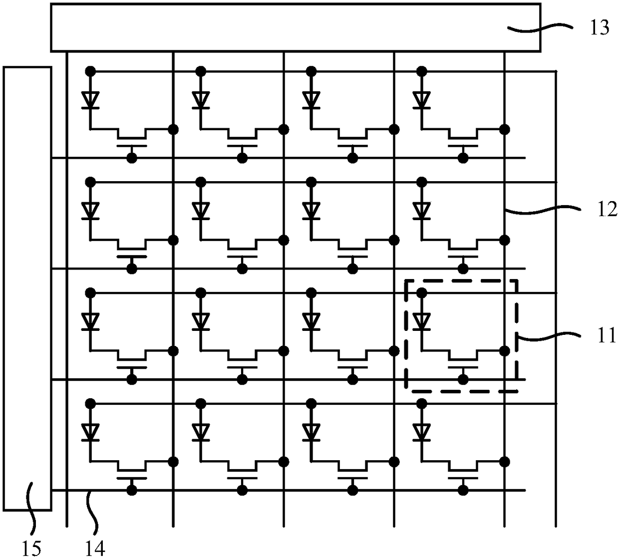
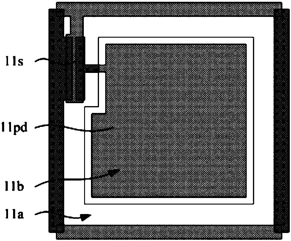
[0061] reference figure 1 with figure 2 ,among them figure 1 Shows a schematic circuit diagram of an image sensor, figure 2 show figure 1 A schematic diagram of the top view structure of a single pixel in the image sensor shown.

[0062] The image sensor is an area array image sensor. Such as figure 1 As shown, the image sensor includes a plurality of pixel units 11, which are arranged in an array to form a pixel array; the pixel units 11 in the same column are connected to the readout circuit 13 through data lines 12 extending in the column direction, The pixel units 11 in the same row are connected to the gate driving circuit 15 through the scan line 14 extending in the row directi...


PUM


Abstract

A fingerprint image module and an electronic device are provided, the fingerprint imaging module comprising a light-shielding dimming layer, the light-shielding dimming layer comprising a light-dimming portion, and a distance between adjacent light-dimming portions increases as a distance from the light source increases; or the light-shielding dimming layer includes a dimming group composed of a plurality of dimming portions, and the spacing between adjacent dimming portions in the dimming group increases as the distance between the dimming group and the light source increases. The setting ofthe light-shielding dimming layer can effectively reduce the difference of the photosensitivity at different positions of the pixel array, is favorable to the improvement of the uniformity of the photosensitivity within the whole pixel array range, and is favorable to the improvement of the fingerprint image quality.

Description

Technical field [0001] The invention relates to the field of fingerprint imaging, in particular to a fingerprint imaging module and electronic equipment. Background technique [0002] Fingerprint recognition is to compare the fingerprint image with the fingerprint information in the fingerprint recognition system after collecting the fingerprint image of the human body to realize identity recognition. Due to the convenience of use and the uniqueness of human fingerprints, fingerprint recognition technology has been widely used in various fields, such as: public security bureaus, customs and other security inspection fields, building access control systems, and consumer products such as personal computers and mobile phones. [0003] One of the fingerprint imaging technologies used in fingerprint recognition is to collect human fingerprint images by optical methods: incident light is generated by a light source; incident light is projected to the surface of the finger, and reflected ...

Claims


Application Information

Patent Timeline
Patent Type & Authority Applications(China)
IPC IPC(8): G06K9/00G06K9/20
CPCG06V40/1324G06V40/1318G06V10/141G06V10/145
Inventor 郑娅洁朱虹凌严吴磊
Owner SHANGHAI OXI TECH
Why Eureka
Try Eureka