Scribing method of power chip and semiconductor device

A power chip and dicing technology, which is applied in semiconductor/solid-state device manufacturing, electrical components, circuits, etc., can solve the problems of edge chipping on the front and back sides of the chip, and achieve the effect of improving the withstand voltage level and reducing the cutting strength

Active Publication Date: 2019-03-08
GLOBAL ENERGY INTERCONNECTION RES INST CO LTD
View PDF10 Cites 10 Cited by
  • Summary
  • Abstract
  • Description
  • Claims
  • Application Information

AI Technical Summary

Problems solved by technology

[0005] In view of this, an embodiment of the present invention provides a method for dicing a power chip and a semiconductor device to solve the problem that in the prior art, power chips are diced by mechanical cutting, which results in the occurrence of problems at the edges of the front and back sides of the diced chip. The problem of edge collapse

Method used


Image

  • Scribing method of power chip and semiconductor device
  • Scribing method of power chip and semiconductor device
  • Scribing method of power chip and semiconductor device

Examples


Embodiment Construction

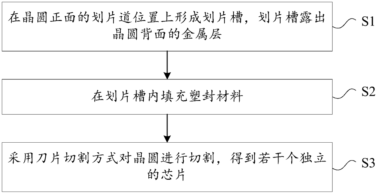
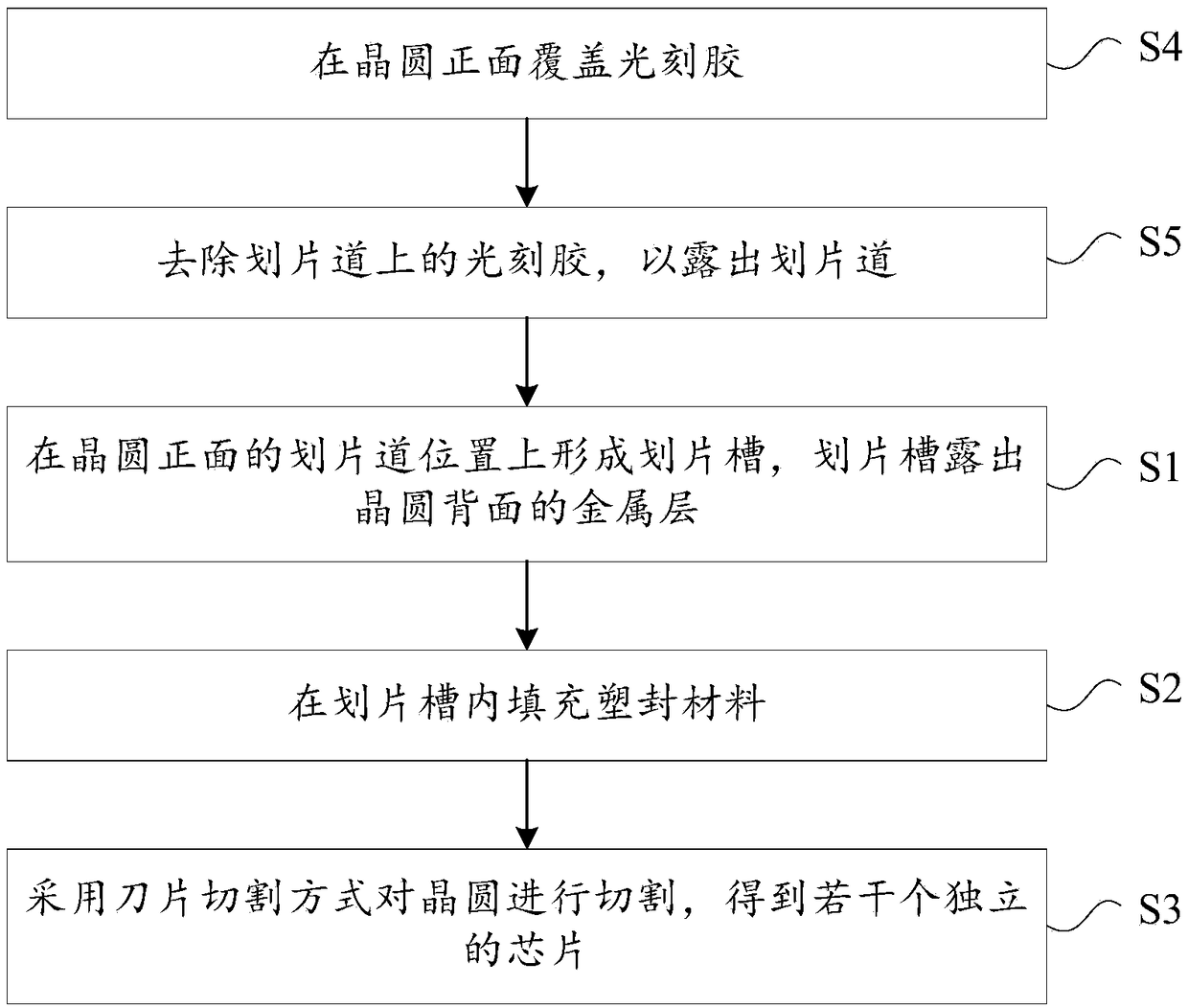
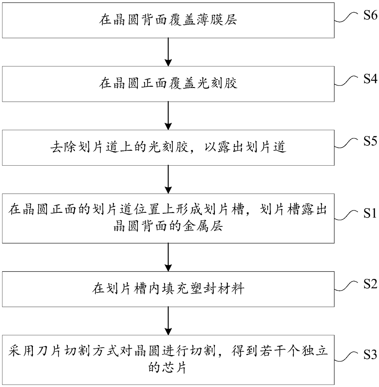
[0029] In order to make the purpose, technical solutions and advantages of the embodiments of the present invention clearer, the technical solutions in the embodiments of the present invention will be clearly and completely described below in conjunction with the drawings in the embodiments of the present invention. Obviously, the described embodiments It is a part of embodiments of the present invention, but not all embodiments. Based on the embodiments of the present invention, all other embodiments obtained by those skilled in the art without creative efforts fall within the protection scope of the present invention.

[0030] In the description of the present invention, it should be noted that the terms "center", "upper", "lower", "left", "right", "vertical", "horizontal", "inner", "outer" etc. The indicated orientation or positional relationship is based on the orientation or positional relationship shown in the drawings, and is only for the convenience of describing the p...


PUM


Abstract

The invention discloses a scribing method of a power chip and a semiconductor device. The scribing method includes following steps: forming scribing grooves at positions of scribing channels on the front surface of a wafer, wherein the scribing grooves expose a metal layer at the backside of the wafer; filling in the scribing grooves with plastic packaging materials; and cutting the wafer by employing a blade cutting mode to obtain a plurality of independent chips. According to the scribing method of the power chip, the scribing grooves are firstly prepared on the front surface of the wafer and extend to the metal layer at the backside of the wafer so that the cutting strength for subsequent mechanical cutting by employing diamond grinding wheel scribing can be greatly reduced; later, theplastic packaging materials are filled in the scribing grooves so that sidewalls of the chips are protected by the plastic packaging materials, and the withstand voltage grade of the chips is improved; and finally, the plurality of independent power chips are obtained by cutting of the wafer through the blade so that the problem of edge breakage at edges of the front surfaces and the backsides ofthe scribed chips due to scribing of the power chips through the mechanical cutting mode in the prior art is solved.

Description

technical field [0001] The invention relates to the technical field of semiconductor packaging, in particular to a method for dicing power chips and a semiconductor device. Background technique [0002] Insulated Gate Bipolar Transistor (IGBT) is a voltage-controlled power electronic device with large input impedance, low drive power, simple control circuit, small switching loss, fast switching speed, high operating frequency, and large component capacity. , no absorption circuit and other advantages, has been widely used in industrial converters, electric traction and other fields. [0003] DC transmission technology can not only be used for long-distance large-capacity power transmission and power system networking, but also can realize submarine cable power transmission and underground cable power transmission in large cities. It is an important technical support for optimal energy allocation and comprehensive utilization. High-voltage direct current transmission (HVDC) ...

Claims


Application Information

Patent Timeline
Patent Type & Authority Applications(China)
IPC IPC(8): H01L21/304H01L21/78
CPCH01L21/3043H01L21/78
Inventor 武伟李现兵韩荣刚吴军民张喆张朋林仲康唐新灵石浩王亮
Owner GLOBAL ENERGY INTERCONNECTION RES INST CO LTD
Why Eureka
Try Eureka