Miniature light emitting diode lamp panel, manufacturing method thereof, backlight module and display device

A technology of light-emitting diodes and manufacturing methods, applied in optics, nonlinear optics, instruments, etc., which can solve the problems of increased etching difficulty, high cost, and reduced pad size

Active Publication Date: 2019-03-08
HISENSE VISUAL TECH CO LTD
View PDF3 Cites 19 Cited by
  • Summary
  • Abstract
  • Description
  • Claims
  • Application Information

AI Technical Summary

Problems solved by technology

[0003] At present, the LED lamp board needs to solder the LED chip on the printed circuit board (PCB for short). The pad size is greatly reduced, resulting in increased etching difficulty
Moreove

Method used


Image

  • Miniature light emitting diode lamp panel, manufacturing method thereof, backlight module and display device
  • Miniature light emitting diode lamp panel, manufacturing method thereof, backlight module and display device
  • Miniature light emitting diode lamp panel, manufacturing method thereof, backlight module and display device

Examples


Embodiment Construction

[0042] In order to make the purpose, technical solutions and advantages of the present invention clearer, the present invention will be further described in detail below in conjunction with the accompanying drawings. Obviously, the described embodiments are only some of the embodiments of the present invention, rather than all of them. Based on the embodiments of the present invention, all other embodiments obtained by persons of ordinary skill in the art without making creative efforts belong to the protection scope of the present invention.

[0043] The micro-LED light panel provided by the specific embodiments of the present invention, its manufacturing method, backlight module and display device will be described in detail below with reference to the accompanying drawings.

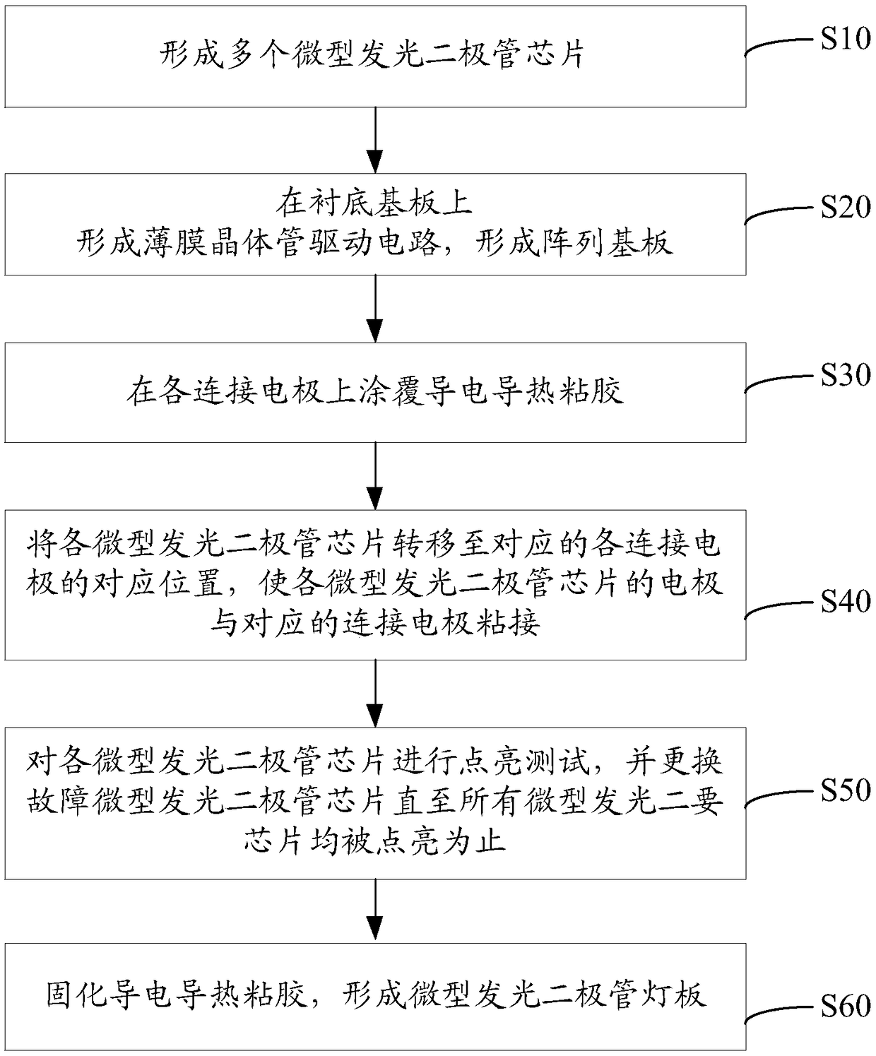
[0044] The first aspect of the embodiments of the present invention provides a method for manufacturing a miniature light-emitting diode lamp panel, such as figure 1 As shown, the above-mentioned manuf...


PUM


Abstract

The invention discloses a miniature light emitting diode lamp panel, a manufacturing method thereof, a backlight module and a display device. A thin film transistor array substrate is used to replacea PCB (Printed Circuit Board) in the prior art. The thin film transistor is characterized in that a large scale semiconductor integrated circuit is manufactured on a glass substrate, and film layers of a generation circuit are formed by sputtering, chemical vapor deposition and other processes, so that the manufacturing cost is lowered, and the etching accuracy is much higher than that of the PCB.During manufacturing of the lamp panel through combination of the thin film transistor array substrate and a miniature light emitting diode chip, the miniature light emitting diode chip is bonded with a current-conducting and heat-conducting adhesive, so that the chip with a poor light emitting effect can be replaced; maintenance of lamp panel is facilitated; and the difficulty of maintenance islowered.

Description

technical field [0001] The invention relates to the field of display technology, in particular to a micro light-emitting diode lamp panel, a manufacturing method thereof, a backlight module and a display device. Background technique [0002] Mini-Light Emitting Diode (Mini LED for short) technology refers to LED technology with a light-emitting chip area size of 100-200 μm. Mini LED inherits the high efficiency, high brightness, high reliability, and fast response time of inorganic LEDs, and has the characteristics of self-illumination without backlight, and has the advantages of energy saving, simple mechanism, small size, and thin profile. It has the advantages of longer luminous life, higher brightness, better material stability, and no image burn-in. Applying it to the backlight module can realize multi-regional dimming of the display device to improve the performance of the display device. display effect. [0003] At present, the LED lamp board needs to solder the LED...

Claims


Application Information

Patent Timeline
IPC IPC(8): H01L33/00H01L27/15H01L33/62G02F1/13357
CPCG02F1/133603H01L27/156H01L33/0095H01L33/62
Inventor 刘振国
Owner HISENSE VISUAL TECH CO LTD
Why Eureka
Try Eureka