sige/ge/sige double heterojunction laser and its preparation method

A double heterojunction and laser technology, applied in the field of semiconductors, can solve the problems of low luminous efficiency and high threshold current density of lasers, and achieve the effect of reducing process difficulty, reducing threshold current density, and simple process

Active Publication Date: 2019-10-29
XIDIAN UNIV
View PDF4 Cites 0 Cited by
  • Summary
  • Abstract
  • Description
  • Claims
  • Application Information

AI Technical Summary

Problems solved by technology

[0006] The laser made with this structure has the defects of too low luminous efficiency and too high threshold current density

Method used


Image

  • sige/ge/sige double heterojunction laser and its preparation method
  • sige/ge/sige double heterojunction laser and its preparation method
  • sige/ge/sige double heterojunction laser and its preparation method

Examples


Embodiment 1

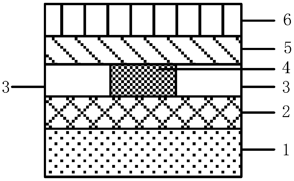
[0041]Based on the defects of low luminous efficiency and high threshold current density in traditional Ge-based lasers, it is very meaningful to study heterojunction structures based on modified Ge. The technical problem of semiconductor Ge-based laser research is how to obtain low threshold current density and high energy conversion efficiency, while improving beam quality and having good spectral characteristics. With the development and progress of material growth and device preparation process. The performance of semiconductor Ge-based lasers has been continuously improved, and the optoelectronic integration of Ge-based lasers can be realized in the near future. The significance of the research of the present invention is to obtain a novel laser structure based on SiGe / Ge / SiGe double heterojunction. Therefore, it is possible to focus on improving the threshold current density and efficiency and reducing optical loss to design a Ge-based laser with higher performance.

...

Embodiment 2

[0061] In the SiGe / Ge / SiGe double heterojunction laser of this embodiment, the molar composition of Ge in SiGe is 0.5, and the molar composition of Ge in Si is 0.5; that is, the SiGe material in the SiGe / Ge / SiGe double heterojunction laser specifically Si 0.5 G 0.5 . The determination of this component is based on the main part of the device structure, that is, the parameters such as the forbidden band width, thickness and doping concentration of each layer of the SiGe / Ge / SiGe double heterojunction, combined with software simulation analysis, and the results obtained after repeated optimization . Experiments have shown that Si 0.5 G 0.5 The material can optimize the lattice mismatch, refractive index, bandgap, etc. required by the SiGe / Ge / SiGe double heterojunction.

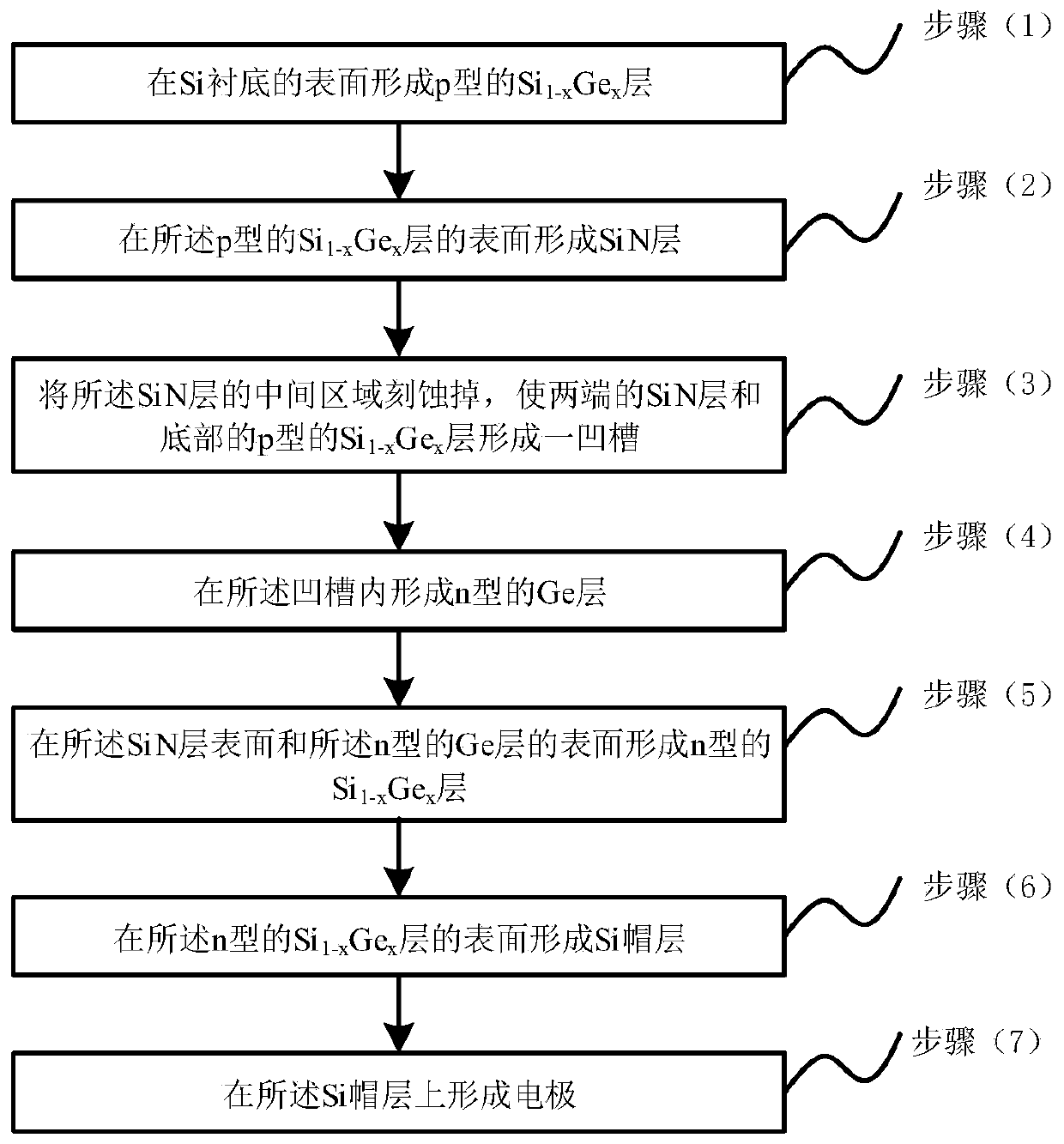
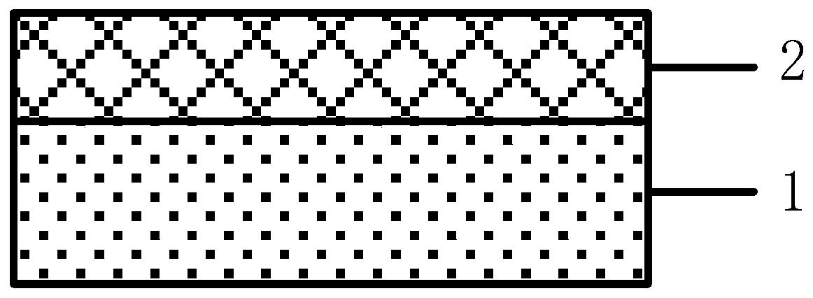
[0062] See 3(a) to 3(f), and figure 1 In this embodiment, on the basis of the above-mentioned embodiments, the preparation method of the SiGe / Ge / SiGe double heterojunction laser and the prepared SiGe / Ge / SiG...


PUM

PropertyMeasurementUnit
thicknessaaaaaaaaaa

Abstract

The invention discloses a SiGe / Ge / SiGe double heterojunction laser and a preparation method thereof. The method comprises the steps that a p-type Si1-xGex layer is formed on the surface of a Si substrate; a SiN layer is formed on the surface of the p-type Si1-xGex layer; the middle area of the SiN layer is removed through etching to enable the two ends of the SiN layer and the bottom p-type Si1-xGex layer to form a groove; an n-type Ge layer is formed in the groove, wherein the thickness of the n-type Ge layer and the thickness of the SiN layer are the same; an n-type Si1-xGex layer is formedon the surface of the SiN layer and the surface of the n-type Ge layer; a Si cap layer is formed on the surface of the n-type Si1-xGex layer; and an electrode is formed on the Si cap layer. The SiGe / Ge / SiGe double heterojunction laser has the high photoelectric conversion efficiency and the low threshold current density and is good in photostability; and the preparation method of the SiGe / Ge / SiGedouble heterojunction laser can be compatible with a CMOS process, processing is easy and convenient, and a specific structure and implementation scheme is provided for achieving an on-chip light source.

Description

technical field [0001] The invention belongs to the technical field of semiconductors, and in particular relates to a SiGe / Ge / SiGe double heterojunction laser and a preparation method thereof. Background technique [0002] At present, due to the constraints of process preparation technology and Si-based materials themselves, the development of monolithic optoelectronic integration is mainly concentrated on III-V materials. However, due to the high cost of epitaxial growth and device manufacturing of III-V materials, its application range is relatively narrow, and large-scale mass production cannot be carried out. However, Si-based materials can greatly reduce the preparation cost by using the existing process line, and have broader application prospects. Ge, which is also a group IV element, has become a hot spot in the research of Si-based luminescence in recent years because it is fully compatible with the Si process. Ge is a quasi-direct bandgap semiconductor, and its d...

Claims


Application Information

Patent Timeline
Patent Type & Authority Patents(China)
IPC IPC(8): H01S5/32H01S5/30
CPCH01S5/3027H01S5/3223
Inventor 舒斌高玉龙张利锋胡辉勇王斌王利明韩本光张鹤鸣
Owner XIDIAN UNIV
Why Eureka
Try Eureka