

Mask plate and making method thereof
A manufacturing method and mask technology, applied in the field of mask, can solve the problems of high scrap rate and low precision, and achieve the effects of reducing scrap rate, improving precision and saving process.
- Summary
- Abstract
- Description
- Claims
- Application Information
AI Technical Summary
Problems solved by technology
Method used
Image

Examples
Embodiment 1
[0022] This embodiment provides a mask, specifically a variable optical transmittance mask.
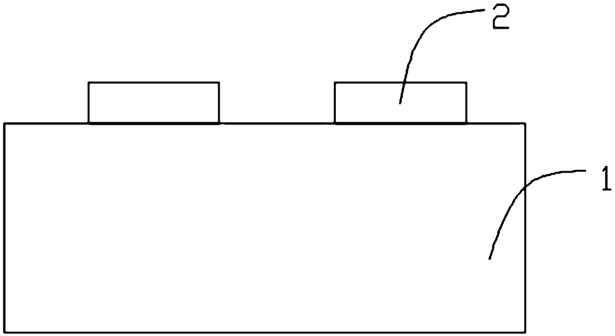
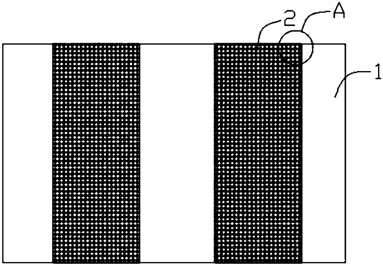
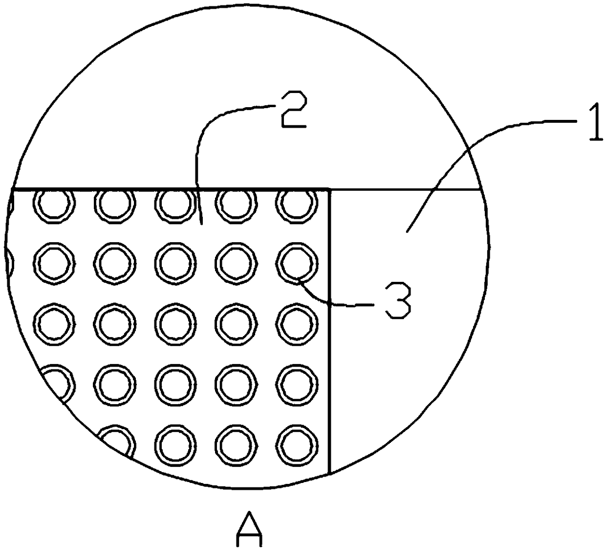
[0023] Please refer to figure 1 , figure 2 and image 3 , the mask plate includes a substrate 1 and a light-blocking layer 2; the light-blocking layer 2 is laid on the substrate 1; a plurality of light-transmitting through-holes 3 are arranged on the light-blocking layer 2, and the light-transmitting through-holes 3 are arranged along a direction perpendicular to the light-blocking layer The direction of 2 penetrates the light-blocking layer 2, and the aperture a of the light-transmitting through hole 3 is: 0.8um≤a≤4um.
[0024] Specifically, within the value range of the aperture of the light-transmitting through-hole 3 , the aperture of the light-transmitting through-hole 3 is proportional to the optical transmittance of the light-blocking layer 2 .
[0025] The aperture of the light-transmitting through hole 3 is smaller than the minimum resolution of the alignment exposure sys...
Embodiment 2
[0038] This embodiment provides a method for manufacturing a mask, which is used to manufacture the mask in Embodiment 1.
[0039] Please refer to Figure 8 , in one embodiment, the manufacturing method of the mask plate includes:
[0040]Step S1 of setting the light-transmitting through-holes: Select the shape, aperture and arrangement density of the light-transmitting through-holes according to the light transmittance of the mask to be produced, and arrange the selected light-transmitting through-holes on a two-dimensional plane to form a light-transmitting through-hole In the hole arrangement area, the aperture of the light-transmitting through-hole is proportional to the optical transmittance of the light-blocking layer, and the arrangement density of the light-transmitting through-hole is proportional to the optical transmittance of the light-blocking layer;
[0041] Graphic fitting step S2: Orthographically project the two-dimensional contour map of the product onto the...
PUM
| Property | Measurement | Unit |
|---|---|---|
| Aperture | aaaaa | aaaaa |
| Thickness | aaaaa | aaaaa |
| Thickness | aaaaa | aaaaa |
Abstract
Description
Claims
Application Information