Cover plate assembly of an embedded touch screen and a manufacturing process of the cover plate assembly

An in-cell touch screen and manufacturing process technology, applied in other home appliances, data processing input/output process, electronic equipment and other directions, can solve problems such as defective bright spots, increase process cost and material cost, improve utilization rate, Guaranteed effect of excellent rate

Pending Publication Date: 2019-03-19
SHENZHEN JUNDA OPTOELECTRONICS
View PDF0 Cites 2 Cited by
  • Summary
  • Abstract
  • Description
  • Claims
  • Application Information

AI Technical Summary

Problems solved by technology

[0007] One of the objects of the present invention is to provide a cover assembly for an in-cell touch screen, so as to solve the technical problem in the prior art that the button structure of the in-cell touch screen has bad bright spots on the back cover when it is lit.

Method used


Image

  • Cover plate assembly of an embedded touch screen and a manufacturing process of the cover plate assembly
  • Cover plate assembly of an embedded touch screen and a manufacturing process of the cover plate assembly
  • Cover plate assembly of an embedded touch screen and a manufacturing process of the cover plate assembly

Examples


specific Embodiment approach

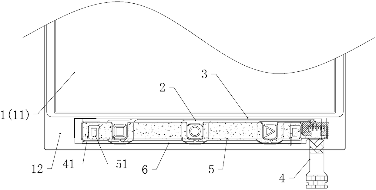
[0069] Print the silver ink on the cover plate 1, the thickness of the silver ink is 6-12μm;

[0070] Bake the silver ink, the baking temperature is 140±5℃, and the time is 60±5min;

[0071] It is beneficial to improve the adhesion of the button circuit 2 and ensure that the adhesion of the button circuit 2 on the cover plate 1 is greater than 4B.

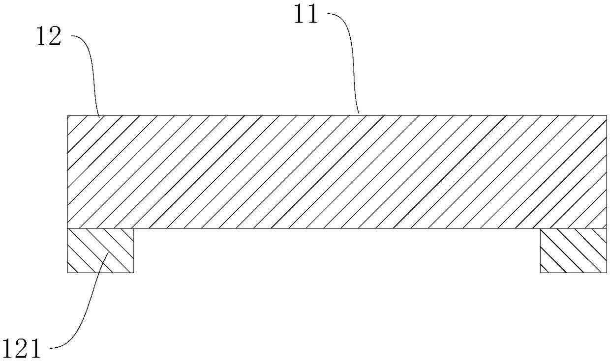
[0072] Further, as a specific embodiment of the manufacturing process of the cover plate assembly of the in-cell touch screen provided by the present invention,

[0073] The printing thickness of insulating ink is 6-18μm;

[0074] The temperature of baking the insulating ink is 120±5℃, and the time is 30±5min;

[0075] It is beneficial to improve the adhesion of the insulating layer 3 and ensure that the adhesion of the insulating layer 3 on the cover plate 1 and the ammonium bond circuit is greater than 4B.

[0076] Further, as a specific implementation of the manufacturing process of the cover assembly of the in-cell touch screen provided by...


PUM

PropertyMeasurementUnit
thicknessaaaaaaaaaa
thicknessaaaaaaaaaa
particle diameteraaaaaaaaaa

Abstract

The invention discloses a cover plate assembly of an embedded touch screen, which comprises a cover plate, a key circuit, an insulating layer, an FPC, a light guide film and a shading film, the key circuit is printed on an ink layer of the cover plate, the insulating layer is printed on the ink layer and covers the key circuit, and the FPC is attached to the insulating layer and electrically connected with the key circuit; the light guide film and the light shielding film are sequentially attached to the FPC, and a light shielding layer is arranged on the face, away from the insulating layer,of the FPC. The invention further discloses a manufacturing process based on the cover plate assembly, including printing silver ink on the cover plate and baking to obtain the key circuit; printing insulating ink and baking to obtain an insulating layer; laminating an FPC on the insulating layer and binding a joint of the key circuit with the FPC, wherein a copper foil at the light shielding layer is reserved when the FPC is manufactured; attaching a light guide film on the FPC; and attaching a shading film to the light guide film. The light shielding layer is laid under the light source, opposite to the light guide film, of the FPC, when the key structure is lightened, the light source is prevented from directly irradiating the cover plate, and therefore the problem of poor bright spotsappearing on the cover plate is avoided.

Description

Technical field [0001] The invention belongs to the technical field of touch screens, and specifically relates to a cover plate assembly of an in-cell touch screen and a manufacturing process thereof. Background technique [0002] The development of mobile phones increasingly tends to be embedded (On-cell / In-cell) touch screens, and Touch Sensors are made on display modules. [0003] The traditional film structure (GF / GFF, etc.) touch screen, ITO Film (ie, ITO film) covers the button position, and the visible area and the touch sensor at the button are directly made on the same ITO Film, without the need for a separate FPC (flexible circuit board). [0004] The in-cell touch screen is difficult to realize the touch function of the buttons at the bottom of the mobile phone. It cannot replicate the button scheme of the traditional film structure touch screen. Because the in-cell touch screen Touch Sensor is made on the display module, there is no need to use ITO Film to stick to the co...

Claims


Application Information

Patent Timeline
Patent Type & Authority Applications(China)
IPC IPC(8): G06F3/041B32B15/04B32B15/20B32B7/12B32B33/00
CPCG06F3/0412B32B7/12B32B15/04B32B15/20B32B33/00B32B2307/206B32B2307/41B32B2307/412B32B2457/208G06F2203/04103
Inventor 谢仰彬黎美锋王令
Owner SHENZHEN JUNDA OPTOELECTRONICS
Why Eureka
Try Eureka