Supercharge Your Innovation With Domain-Expert AI Agents!

Cooling unit, heat insulating structure, substrate processing apparatus, and manufacturing method of semiconductor device

A technology for a substrate processing device and a cooling unit, which is used in semiconductor/solid-state device manufacturing, furnace cooling, electrical components, etc., can solve problems such as temperature change differences, and achieve the effect of improving responsiveness

Active Publication Date: 2022-05-17
KOKUSA ELECTRIC CO LTD
View PDF7 Cites 0 Cited by
  • Summary
  • Abstract
  • Description
  • Claims
  • Application Information

AI Technical Summary

Problems solved by technology

However, in the above-mentioned cooling unit structure, the reaction tube cannot be cooled uniformly in the rapid cooling by controlling the flow rate of the cooling gas, so the cooling rate will vary with the change of the area, resulting in differences in the temperature change process between the areas.

Method used


Image

  • Cooling unit, heat insulating structure, substrate processing apparatus, and manufacturing method of semiconductor device
  • Cooling unit, heat insulating structure, substrate processing apparatus, and manufacturing method of semiconductor device
  • Cooling unit, heat insulating structure, substrate processing apparatus, and manufacturing method of semiconductor device

Examples


Embodiment Construction

[0028] One embodiment of the present invention will be described below with reference to the drawings.

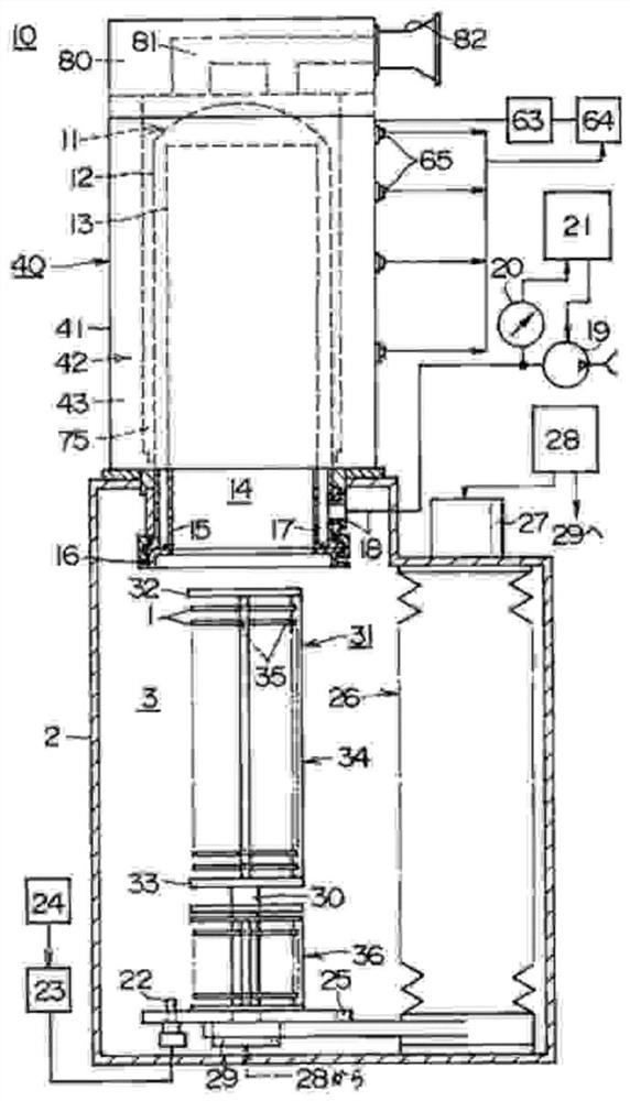
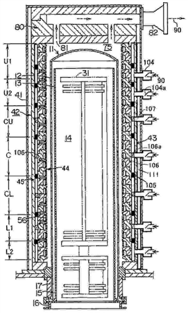
[0029] In this embodiment, if figure 1 and figure 2 As shown, the substrate processing apparatus 10 of the present invention is configured as a processing apparatus 10 for performing a film forming step in a semiconductor device manufacturing method.

[0030] figure 1 The illustrated substrate processing apparatus 10 includes a processing tube 11 as a supported vertical reaction tube, and the processing tube 11 is composed of an outer tube 12 and an inner tube 13 arranged concentrically with each other. Outer tube 12 uses quartz (SiO 2 ) is integrally formed into a cylindrical shape with the upper end closed and the lower end open. The inner tube 13 is formed in a cylindrical shape with upper and lower ends opened. The hollow portion of the inner tube 13 forms a processing chamber 14 into which a wafer boat described later is carried in, and the lower end opening of t...


PUM


Abstract

The present invention relates to a cooling unit, a heat insulating structure, a substrate processing apparatus, and a method of manufacturing a semiconductor device, and provides a structure that improves the responsiveness of heating and cooling control between regions. It is configured to include: a suction pipe provided in each area to supply gas for cooling the reaction tube; a control valve provided in the suction pipe to adjust the flow rate of the gas; and temporarily storing the gas supplied from the suction pipe. The buffer part that stays; And, be provided with the opening that the gas stored in the buffer part is blown toward the reaction tube, thus provide the flow rate of the gas introduced into the suction pipe by setting the length ratio of the up and down direction of the region, Therefore, the control valve is opened and closed to adjust the flow rate and flow velocity of the gas ejected from the opening toward the reaction tube.

Description

technical field [0001] The present invention relates to a cooling unit, a heat insulating structure, a substrate processing device, and a method of manufacturing a semiconductor device. Background technique [0002] A semiconductor manufacturing apparatus is known as an example of a substrate processing apparatus, and a vertical apparatus is known as an example of a semiconductor manufacturing apparatus. In the vertical apparatus, a wafer boat, which is a substrate holding unit that holds multiple substrates (hereinafter also referred to as wafers) in multiple layers, is carried into the processing chamber in the reaction tube with the substrates held, and the temperature is controlled in multiple regions. control, and process the substrate at a predetermined temperature. Conventionally, in the temperature control of the heater, the heater was turned off when the temperature was lowered, but in recent years, the cooling gas is supplied from the cooling mechanism, and the co...

Claims


Application Information

Patent Timeline
Patent Type & Authority Patents(China)
IPC IPC(8): H01L21/67
CPCH01L21/67098F27B17/0025F27D9/00F27D2009/0005H01L21/67109H01L21/67017H01L21/324H01L21/0262
Inventor 小杉哲也村田等上野正昭
Owner KOKUSA ELECTRIC CO LTD
Features
  • R&D
  • Intellectual Property
  • Life Sciences
  • Materials
  • Tech Scout
  • Unparalleled Data Quality
  • Higher Quality Content
  • 60% Fewer Hallucinations
Learn More