Transferable logic chip based on mechanical peeling and preparation method thereof

A logic chip and mechanical stripping technology, applied in the direction of electrical components, circuits, semiconductor devices, etc., can solve the problems of inability to achieve mass production of devices, poor compatibility, and complicated growth process, and achieve flexible wearable, spectrum utilization rate improvement, The effect of broadening the field of application

Active Publication Date: 2019-03-26
NANJING UNIV OF POSTS & TELECOMM
View PDF4 Cites 2 Cited by
  • Summary
  • Abstract
  • Description
  • Claims
  • Application Information

AI Technical Summary

Problems solved by technology

The use of the sacrificial layer can certainly solve the substrate transfer, but its growth process is complicated, and it is not compatible with the traditional process, so it cannot realize the mass production of the device

Method used


Image

  • Transferable logic chip based on mechanical peeling and preparation method thereof
  • Transferable logic chip based on mechanical peeling and preparation method thereof
  • Transferable logic chip based on mechanical peeling and preparation method thereof

Examples


Embodiment Construction

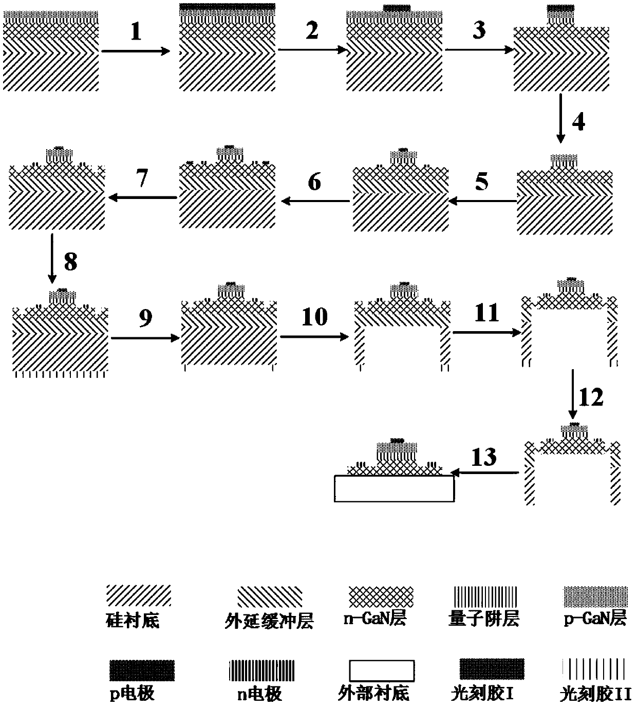
[0036] The present invention will be further described below in conjunction with embodiment and accompanying drawing.

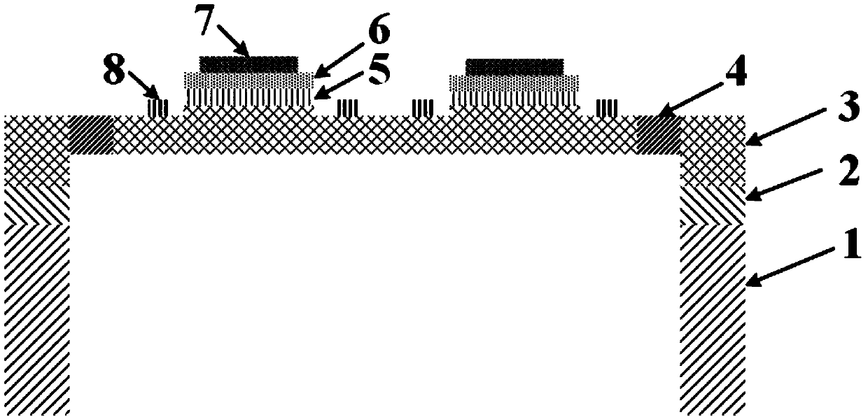
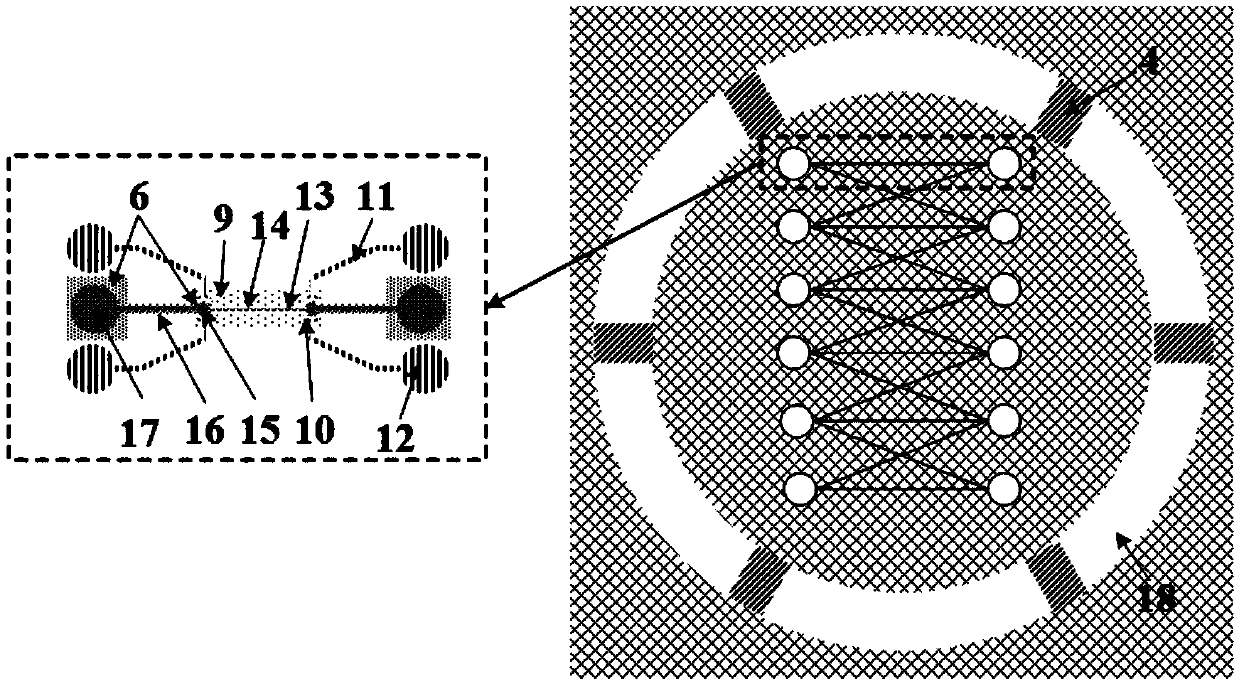
[0037] figure 1 , figure 2 Front and top views of the micron-scale transferable logic chip based on mechanical lift-off of the present invention are given.

[0038]The chip uses silicon substrate nitride as a carrier, and includes an epitaxial buffer layer 2 on a silicon substrate layer 1, an n-GaN layer 3 disposed on the epitaxial buffer layer 2, and an n-GaN layer disposed on the n-GaN layer 3. Multiple pairs of suspended p-n junction quantum well devices and suspended waveguides; the p-n junction quantum well devices include, from bottom to top, n-electrode 8 on n-GaN layer 3, InGaN / GaN multiple quantum wells 5 and the p-GaN layer 6 and p-electrode 7 on the GaN multiple quantum well 5 . A cavity is provided below the n-GaN layer 3 through the silicon substrate layer 1, the epitaxial buffer layer 2 to the n-GaN layer 3, so that the p-n junction quantum ...


PUM


Abstract

The invention discloses a transferable logic chip based on mechanical stripping and a preparation method thereof. The logic chip comprises a plurality of pairs of p-n junction quantum wells and a suspended GaN waveguide connected between the p-n junction quantum wells. A logical AND operation and a logical OR operation can be implemented between the plurality of pairs of p-n junction quantum wells. The p-n junction quantum wells can transmit optical signals to the outside and detect optical signals in the space, which means that the p-n junction quantum wells can detect the optical signals inthe space while emitting light, and the full-duplex communication is achieved. According to the invention, a transferable logic film chip is achieved for the first time by using the traditional semiconductor processing technology, after a device is stripped, the device is transferred to a flexible carrier, and the chip can be used in the fields of communication, illumination, intelligent display,logic operation and sensing.

Description

technical field [0001] The invention belongs to the field of information materials and devices, and relates to a transferable logic chip and its preparation technology. Background technique [0002] At present, as far as InGaN / GaN multi-quantum well materials are concerned, there are mainly three transfer methods: laser lift-off, mechanical lift-off and chemical etching. Laser lift-off is to use laser to directly remove the substrate of the LED wafer, and then transfer the LED to other substrates. This method is convenient and simple to use. It is often used on sapphire substrates, but it is easy to cause damage to the LED, affecting its threshold voltage and light output. efficiency. Chemical etching first needs to grow a sacrificial layer that is easy to peel off on the initial substrate, grow the LED structure on the sacrificial layer, and transfer the LED structure through the sacrificial layer that is easy to peel off under the action of an external force. This method ...

Claims


Application Information

Patent Timeline
Patent Type & Authority Applications(China)
IPC IPC(8): H01L33/02H01L33/00
CPCH01L33/0093H01L33/02
Inventor 施政王永进蒋燕高绪敏袁佳磊
Owner NANJING UNIV OF POSTS & TELECOMM
Why Eureka
Try Eureka