Silicon wafer automatic coating source production line

A technology of production line and silicon wafer, applied in the direction of electrical components, semiconductor/solid-state device manufacturing, circuits, etc., can solve the problems of low manual coating efficiency, high manual operation error rate, uneven quality of coating, etc., and achieve coating efficiency High, high degree of automation, low error rate effect

Active Publication Date: 2019-04-02
TIANJIN HUANXIN TECH DEV
View PDF12 Cites 0 Cited by
  • Summary
  • Abstract
  • Description
  • Claims
  • Application Information

AI Technical Summary

Problems solved by technology

In the process of semiconductor silicon wafer production, it is necessary to coat the diffusion source on the silicon wafer to form a PN junction. However, in the prior art, manual coating is often used to complete the process. Since the production of silicon wafers involves a variety of work processes, resulting in product Efficiency and quality need to be improved. At present, there are manual coating operation methods: high error rate in manual operation; special personnel are required to operate; manual coating efficiency is low. Therefore, in order to solve the uneven quality of coating caused by manual coating The problem is that an automatic equipment is needed to realize the automatic coating function of circular silicon wafers, so that the silicon wafers can be evenly coated, avoiding unqualified products caused by personnel problems, and achieving stable and efficient output

Method used


Image

  • Silicon wafer automatic coating source production line
  • Silicon wafer automatic coating source production line
  • Silicon wafer automatic coating source production line

Examples


Embodiment Construction

[0060] Embodiments of the present invention are further described below in conjunction with the accompanying drawings:

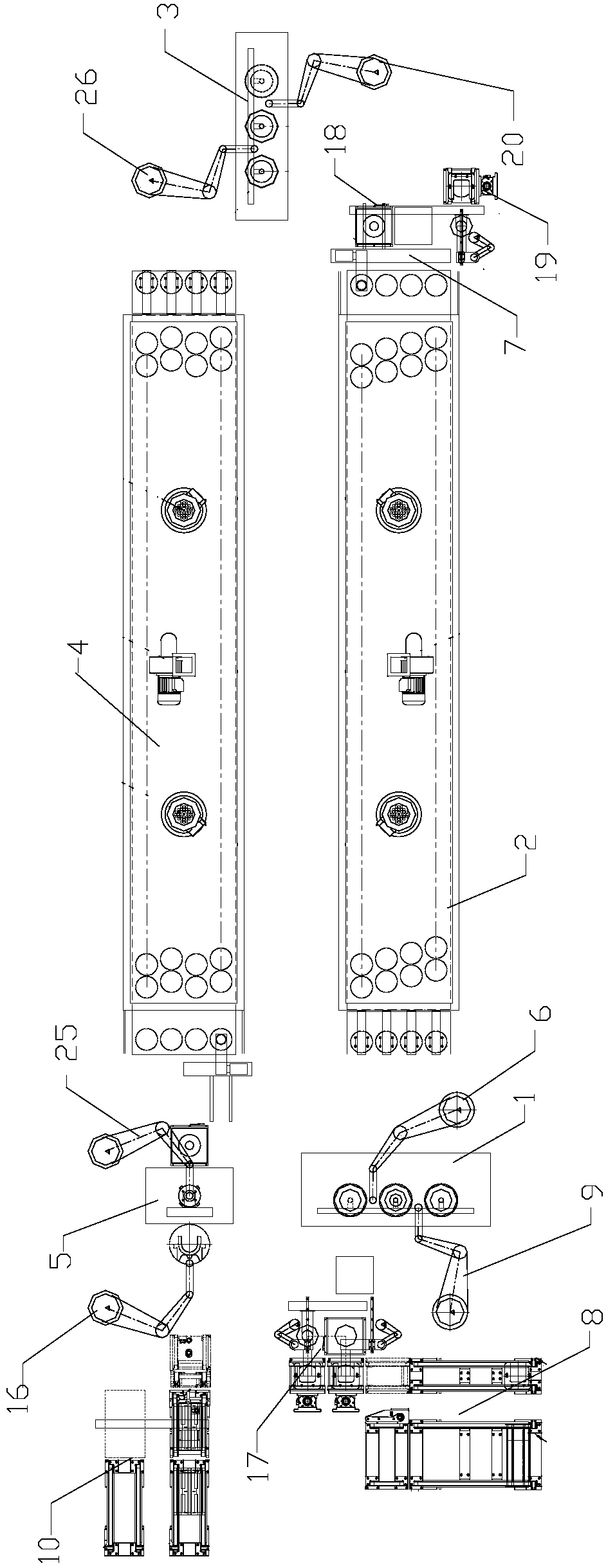
[0061] like figure 1As shown, a kind of silicon wafer automatic source coating production line described in the present embodiment comprises a boron coating device 1, a drying furnace 2, a phosphorus coating device 3, a drying furnace 4 and a powder spreading unit 5, and the boron coating device 1 and the drying furnace Between the drying furnace 2, between the drying furnace 2 and the phosphorus coating device 3, between the phosphorus coating device 3 and the drying furnace 4, between the drying furnace 4 and the powdering unit 5, there are transfer manipulators, and the drying furnace The downstream end of 2 is provided with silicon wafer turnover mechanism 7. After the boron diffusion source is sprayed on the silicon wafer in the boron coating device 1, it is transferred to the drying furnace 2 by the transfer manipulator 6, and the side sprayed with th...


PUM


Abstract

The invention provides a silicon wafer automatic coating source production line. The silicon wafer automatic coating source production line comprises a boron coating device, a first drying furnace, aphosphorus coating device, a second drying furnace and a powder spraying unit, first transfer manipulators are arranged between the boron coating device and the first drying furnace, between the firstdrying furnace and the phosphorus coating device, between the phosphorus coating device and the second drying furnace and between the second drying furnace and the powder spraying unit, and one end of the downstream of the first drying furnace is provided with a silicon wafer turnover mechanism. The silicon wafer automatic coating source production line is high in automatic degree, multiple processes of the silicon wafer coating sources are automatically performed with no need for equipping with a lot of special manual operation, the failure rate is low, the coating efficiency is high, the coating is uniform, and the product qualification rate is high.

Description

technical field [0001] The invention belongs to the field of silicon wafer production equipment, and in particular relates to an automatic coating source production line for silicon wafers. Background technique [0002] With the rapid development of the semiconductor industry, the production capacity of semiconductor silicon wafers is expanding day by day. In the process of semiconductor silicon wafer production, it is necessary to coat the diffusion source on the silicon wafer to form a PN junction. However, in the prior art, manual coating is often used to complete the process. Since the production of silicon wafers involves a variety of work processes, resulting in product Efficiency and quality need to be improved. At present, there are manual coating operation methods: high error rate in manual operation; special personnel are required to operate; manual coating efficiency is low. Therefore, in order to solve the uneven quality of coating caused by manual coating The p...

Claims


Application Information

Patent Timeline
Patent Type & Authority Applications(China)
IPC IPC(8): H01L21/67
CPCH01L21/6715
Inventor 董文一魏文博钟瑜徐长坡陈澄梁效峰杨玉聪甄辉齐风李亚哲黄志焕王晓捧王宏宇王鹏徐艳超
Owner TIANJIN HUANXIN TECH DEV
Why Eureka
Try Eureka