Turnover device for diode package

A flipping device, diode technology, applied in the direction of electrical components, semiconductor/solid-state device manufacturing, circuits, etc., to achieve the effect of improving production efficiency, ensuring production quality, and improving processing accuracy

Active Publication Date: 2019-04-02
TIANJIN TIANXING ELECTRONICS
View PDF3 Cites 6 Cited by
  • Summary
  • Abstract
  • Description
  • Claims
  • Application Information

AI Technical Summary

Problems solved by technology

[0006] The main purpose of the present invention is to solve the problems existing in the prior art, to provide a simple structure, which can realize the integral packaging and molding of the bottom material, chip and cover material in the diode packaging process, and effectively avoid manual or semi-manual packaging. Those who are easily affected by external factors have paste deviation problems, so as to ensure the quality of packaging processing, improve production efficiency, and reduce labor intensity. The flipping device for diode packaging

Method used


Image

  • Turnover device for diode package
  • Turnover device for diode package
  • Turnover device for diode package

Examples


Embodiment Construction

[0032] In order to better understand the present invention, the present invention will be further described below in conjunction with specific embodiments and accompanying drawings.

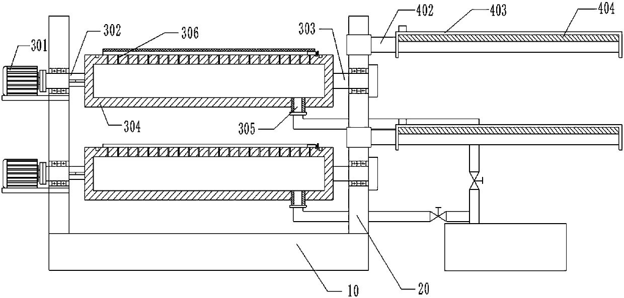
[0033] Such as Figure 1-Figure 8As shown, a flipping device for diode packaging includes a base 10, a column 20, a packaging process 1 30, a baking mechanism 40, a packaging process 2 50, and a baking mechanism 2 60, and the base 10 is vertically and correspondingly arranged Two upright columns 20, between the two upright columns 20 are arranged horizontally from top to bottom sequentially a baking mechanism 1 40, a packaging process 1 30, a baking mechanism 2 60 and a packaging process 2 50, and the two ends of the packaging process 1 30 and the packaging process 2 50 Both are installed on the two uprights 20, and the packaging process 1 30 and the packaging process 2 50 can be rotated 180 degrees, and the ends of the baking mechanism 1 40 and the baking mechanism 2 60 are both set on the right...


PUM


Abstract

The invention provides a turnover device for diode package. The turnover device comprises a base, columns, a packaging process 1, a baking mechanism 1, a packaging process 2 and a baking mechanism 2.The two columns are vertically and oppositely arranged on the base, the baking mechanism 1, the packaging process 1, the baking mechanism 2 and the packaging mechanism 2 are horizontally arranged between the two columns from top to bottom, the two ends of the packaging process 1 and the packaging process 2 penetrate the two columns, the packaging process 1 and the packaging process 2 can be rotated for 180 degrees, one ends of the baking mechanism 1 and the baking mechanism 2 sleeve the column at the right side, and the baking mechanism 1 and the baking mechanism 2 can be rotated for 180 degrees around the column at the right side. The turnover device for diode package can achieve integrated packaging and forming of the bottom material piece, the chip and the cover material piece in the diode package process so as to effectively avoid the problem that the three are prone to external factor influences to generate paste deviation when artificial and semi-artificial package is performed,ensure the package processing quality and improve the product efficiency.

Description

technical field [0001] The invention relates to the technical field of auxiliary equipment for diode packaging, in particular to a flipping device for diode packaging. Background technique [0002] At present, the packaging of diodes not only plays the role of installation, fixing, sealing, protecting the chip and enhancing the electrothermal performance, but also connects the contacts on the chip to the pins of the package shell with wires, and these pins are printed. The wires on the circuit board are connected to other devices, so as to realize the connection between the internal chip and the external circuit. The packaged chip can effectively prevent the external air from corroding the chip circuit, and makes the chip easy to install and transport. In the packaging process of the diode, bonding the chip between the cover and the bottom sheet of the diode is a very important process. In order to realize the packaging of chips in diodes, manual or semi-manual methods are...

Claims


Application Information

Patent Timeline
Patent Type & Authority Applications(China)
IPC IPC(8): H01L21/67H01L21/68H01L21/683
CPCH01L21/67121H01L21/68H01L21/6838
Inventor 曹锡文李晓辉石海莲王蔚
Owner TIANJIN TIANXING ELECTRONICS
Why Eureka
Try Eureka