TO packaging-based semiconductor laser and packaging method thereof

A packaging method and laser technology, which is applied in the direction of semiconductor lasers, lasers, laser components, etc., can solve the problems of poor interchangeability of components, low reliability, and high cost of use

Active Publication Date: 2019-04-05
深圳朗光科技有限公司
View PDF6 Cites 0 Cited by
  • Summary
  • Abstract
  • Description
  • Claims
  • Application Information

AI Technical Summary

Problems solved by technology

[0003] The object of the present invention is to provide a semiconductor laser based on TO packaging, which is used to solve the problem of low material reutilization rate and poor interchangeability of original parts of TO packaging semiconductor lasers in the prior art, resulting in poor final reliability. Technical issues with high and high cost of use

Method used


Image

  • TO packaging-based semiconductor laser and packaging method thereof
  • TO packaging-based semiconductor laser and packaging method thereof
  • TO packaging-based semiconductor laser and packaging method thereof

Examples


Embodiment Construction

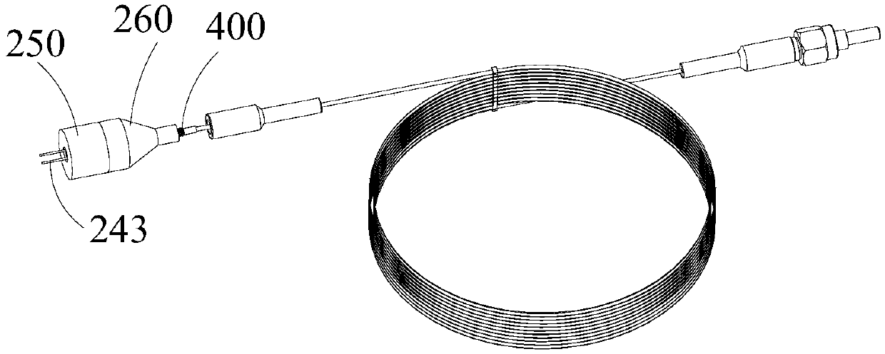
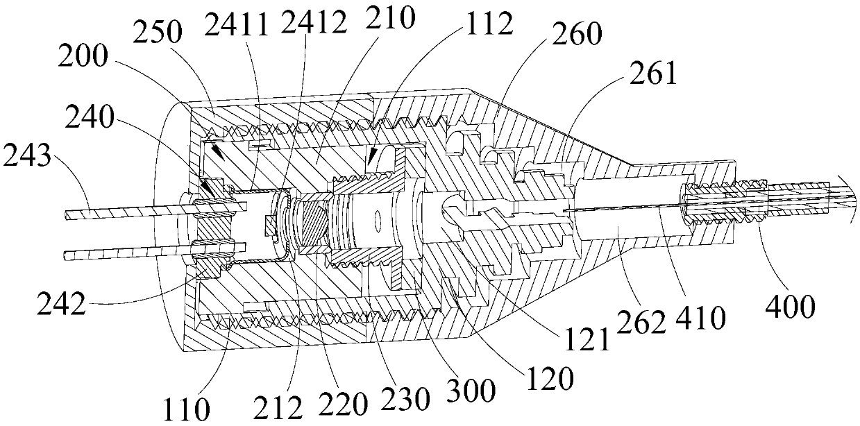
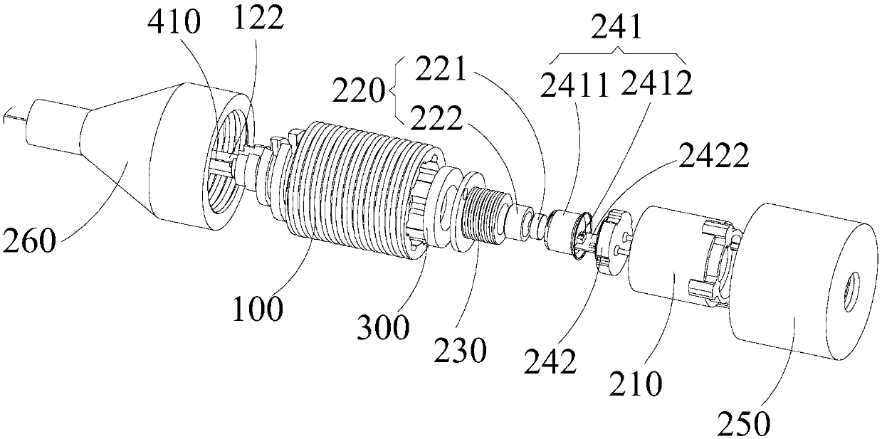
[0043] In order to make the technical problems, technical solutions and beneficial effects to be solved by the present invention clearer, the following further describes the present invention in detail with reference to specific drawings and specific embodiments. Wherein, the same or similar reference signs in the drawings of the specific embodiments of the present invention represent the same or similar elements, or elements with the same or similar functions. It should be understood that the specific embodiments described below are intended to explain the present invention, but not to limit the present invention.

[0044] It should be noted that when an element is referred to as being "fixed on" or "mounted on" or "disposed on" or "connected to" another element, it can be directly or indirectly located on the other element. For example, when an element is referred to as being "connected to" another element, it can be directly or indirectly connected to the other element. The t...


PUM


Abstract

The invention belongs to the technical field of laser manufacturing, and aims to provide a TO packaging-based semiconductor laser and a packaging method thereof. The semiconductor laser comprises a base cylinder, a focusing assembly, a packaging rear cylinder and a TO packaging assembly comprising a light-emitting assembly; in the axial direction of the base cylinder, a mounting groove is formed in an inserting-connecting portion of the base cylinder; a coupling part is provided with a light outlet hole which is communicated with the mounting groove and is connected with an optical fiber in aninserted mode; and the light beam emitted by the light emitting assembly is focused by the focusing assembly and then can be coupled into the optical fiber to be output from the light outlet hole. During packaging, the focusing assembly is firstly inserted into the mounting groove from the axial direction and is limited on the base cylinder in the circumferential direction, and then the TO packaging assembly is inserted into a positioning cylinder of the focusing assembly and is limited on the positioning cylinder in the circumferential direction; finally, the packaging rear cylinder sleevesthe inserting-connecting portion of the base cylinder in the axial direction and is in spiral connection with the inserting-connecting portion of the base cylinder, so that the focusing assembly and the light-emitting assembly are packaged in the mounting groove of the base cylinder; and therefore, the packaging process is simple, the interchangeability of materials is high, the rejection rate islow, and the reliability is high.

Description

Technical field [0001] The invention belongs to the technical field of laser manufacturing, and more specifically, relates to a semiconductor laser based on TO packaging and a packaging method thereof. Background technique [0002] With the continuous development of science and technology, packaging technologies for semiconductor lasers include butterfly packaging and TO packaging. Among them, TO (Transistor Outline, originally defined as a transistor case) package refers to a coaxial package, which belongs to a fully enclosed package. It is widely used in optoelectronics due to its simple manufacturing process, low production cost, and ease of use. Devices such as laser diode packages. However, the existing manufacturing process of TO packaged semiconductor lasers is often complicated, and requires high professional skills of production personnel. In addition, when the device is repaired, the material reutilization rate is low, and the interchangeability of the original parts ...

Claims


Application Information

Patent Timeline
Patent Type & Authority Applications(China)
IPC IPC(8): H01S5/022
CPCH01S5/02251H01S5/02253H01S5/02325
Inventor 刘守斌
Owner 深圳朗光科技有限公司
Why Eureka
Try Eureka