Multi-single tube large-power semiconductor laser package structure and laser

A packaging structure and laser technology, applied in semiconductor lasers, lasers, laser parts and other directions, can solve the problems of large volume, poor heat dissipation, high material cost and production cost, achieve high laser output power, save packaging space, The effect of reducing material cost

Active Publication Date: 2019-04-05
深圳朗光科技有限公司
View PDF11 Cites 6 Cited by
  • Summary
  • Abstract
  • Description
  • Claims
  • Application Information

AI Technical Summary

Problems solved by technology

[0005] The purpose of the present invention is to provide a package structure of multiple single-tube high-power semiconductor lasers, which is used to solve the problem of large volume,

Method used


Image

  • Multi-single tube large-power semiconductor laser package structure and laser
  • Multi-single tube large-power semiconductor laser package structure and laser
  • Multi-single tube large-power semiconductor laser package structure and laser

Examples


Embodiment Construction

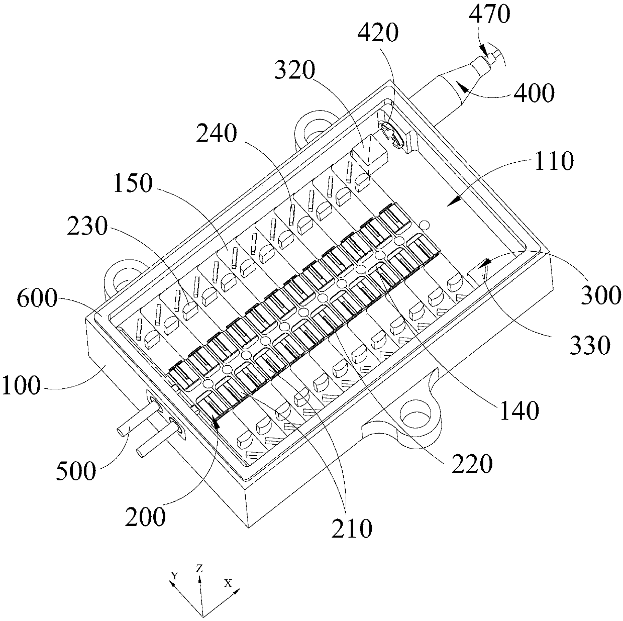
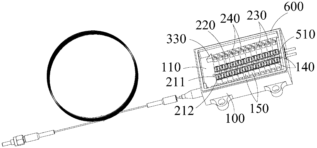
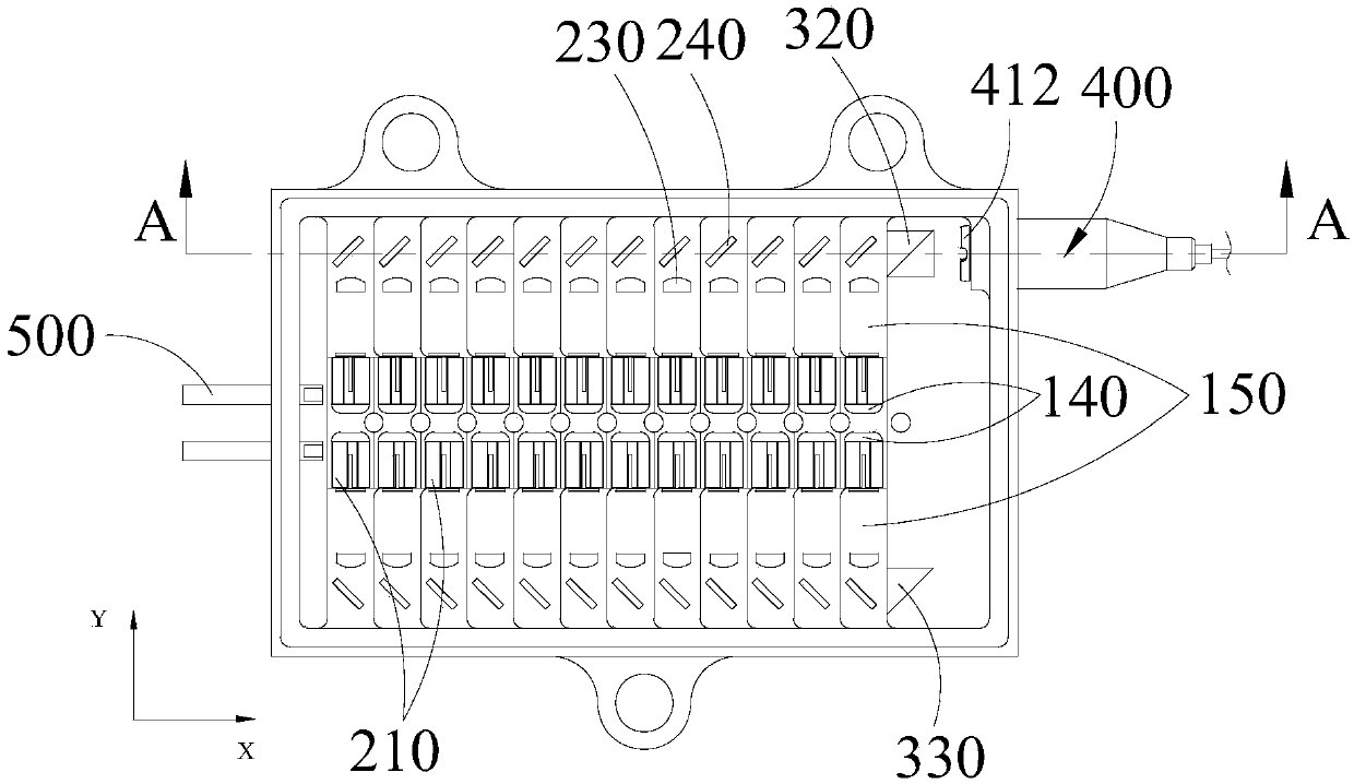
[0039]In order to make the technical problems, technical solutions and beneficial effects to be solved by the present invention clearer, the present invention will be further described in detail below in conjunction with specific drawings and specific embodiments. Wherein, the same or similar symbols in the drawings of the specific embodiments of the present invention indicate the same or similar elements, or elements with the same or similar functions. It should be understood that the specific embodiments described below are intended to explain the present invention, not to limit the present invention.

[0040] It should be noted that when an element is referred to as being “fixed on” or “mounted on” or “provided on” or “connected to” another element, it may be directly or indirectly located on the other element. For example, when an element is referred to as being "connected to" another element, it can be directly or indirectly connected to the other element. The terms "len...


PUM


Abstract

The invention belongs to the technical field of laser manufacturing, and aims to provide a multi-single tube large-power semiconductor laser package structure and a laser. The package structure comprises a base shell, wherein a package groove is formed in the base shell, a plurality of first steps are arranged at a central region of the groove bottom of the package groove and are integratedly formed along an X-axis direction so as to achieve integrated design of the package shell, the material cost and the production cost; and moreover, the height of a step surface of each step along a Z-axisdirection is sequentially and gradually reduced along a positive direction of an X axis, two groups of COS assemblies are arranged on the step surface of the corresponding step in a back-to-back way,and light emitted from each light-emitting unit is converted to collimating parallel light, gathered in the package groove and then is introduced to a light path coupling assembly outside the packagegroove for focusing and coupling. Apparently, the laser forms a new light path and electrical-thermal-mechanical balance, the volume is greatly reduced, concentrated heat dissipation is beneficial forcontrolling the integral temperature, light beam subsequent coupling is small in influence on the light-emitting unit, the output power of the laser is large, and the laser is more stable in performance.

Description

technical field [0001] The invention belongs to the technical field of laser manufacturing, and more specifically relates to a multi-single-tube high-power semiconductor laser packaging structure and a laser. Background technique [0002] A laser is a device capable of emitting laser light. Common semiconductor lasers are widely used in industrial processing, military, medical, security and other fields due to their small size, light weight, high efficiency, and long life. With the vigorous development of fiber lasers, the demand for semiconductor lasers with high power and high beam quality is increasing. At present, there are mainly two types of semiconductor lasers in the market, namely, single-tube semiconductor lasers and multi-single-tube semiconductor lasers. Among them, high-power applications often Using multiple single-tube semiconductor lasers, such as 24-core high-power lasers. However, the existing multi-tube semiconductor lasers mainly have the following defec...

Claims


Application Information

Patent Timeline
IPC IPC(8): H01S5/022
CPCH01S5/02255H01S5/02325
Inventor 刘守斌
Owner 深圳朗光科技有限公司
Why Eureka
Try Eureka