Waveguide core layer, mode spot converter, silicon optical device, and optical communication unit

A mode spot converter and waveguide core technology, applied in the field of optical communication, can solve the problems of high cost, large optical loss, poor channel uniformity, etc., and achieve the effects of precise docking, reducing optical loss, and improving channel uniformity

Inactive Publication Date: 2019-04-19
HUAWEI TECH CO LTD
View PDF11 Cites 4 Cited by
  • Summary
  • Abstract
  • Description
  • Claims
  • Application Information

AI Technical Summary

Problems solved by technology

[0005] The embodiment of the present application provides a waveguide core layer, a mode spot converter, a silicon optical device, and an optical communication device, which solves the p

Method used


Image

  • Waveguide core layer, mode spot converter, silicon optical device, and optical communication unit
  • Waveguide core layer, mode spot converter, silicon optical device, and optical communication unit
  • Waveguide core layer, mode spot converter, silicon optical device, and optical communication unit

Examples


Example Embodiment

[0057] Example one

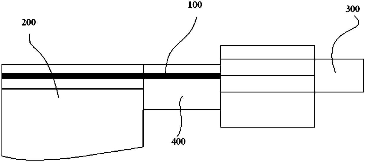
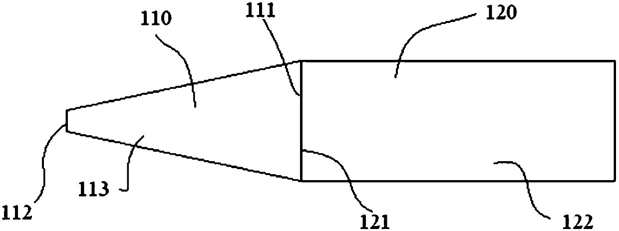
[0058] figure 1 This is a schematic connection diagram of Embodiment 1 of the waveguide core layer of this application; figure 2 for figure 1 Schematic diagram of the overall structure of the middle waveguide core. Please refer to figure 1 with figure 2 , This embodiment provides a waveguide core layer 100, including: a first waveguide region 110 and a second waveguide region 120 connected in a first direction; and the first waveguide region 110 and the second waveguide region 120 are both along the first direction Extension; the end of the first waveguide region 110 away from the second waveguide region 120 is used to connect to the silicon optical chip 200, the end of the second waveguide region 120 away from the first waveguide region 110 is used to connect to the optical fiber 300; the first waveguide region 110 is along The size in the second direction increases from the end away from the second waveguide region 120 to the end close to the second waveg...

Example Embodiment

[0072] Example two

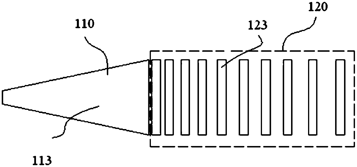
[0073] In this embodiment, the method of changing the refractive index of the second waveguide region 120 is improved on the basis of the first embodiment. For other structures, reference may also be made to the first embodiment, which will not be repeated here. image 3 This is a schematic diagram of the overall structure of Embodiment 2 of the waveguide core layer of this application. image 3 Here, the first direction may be the left-right direction in the figure, the second direction may be the up-down direction in the figure, and the third direction may be a direction perpendicular to the paper surface. Please refer to image 3 , The second waveguide region 120 includes a plurality of second solid waveguide portions 123 arranged at intervals along the first direction, and one of the plurality of second solid waveguide portions 123 close to the first waveguide region 110 has a second cross section 121, and the second cross section 121 is located at an end ...

Example Embodiment

[0079] Example three

[0080] This embodiment is an improvement on the structure of the first waveguide region 110 on the basis of the first or second embodiment. For the structure of the second waveguide region 120, please refer to the first or second embodiment, which will not be repeated here. . Figure 4 This is a schematic diagram of the overall structure of Embodiment 3 of the waveguide core layer of this application. Figure 4 Here, the first direction may be the left-right direction in the figure, the second direction may be the up-down direction in the figure, and the third direction may be a direction perpendicular to the paper surface. Please refer to Figure 4 , The first waveguide region 110 includes: a first sub-waveguide region 114 and a second sub-waveguide region 116 arranged in sequence along the first direction; an end of the second sub-waveguide region 116 away from the first sub-waveguide region 114 and the second waveguide region 120 Connection; the first su...


PUM


Abstract

The invention provides a waveguide core layer, a mode spot converter, a silicon optical device and an optical communication unit. The waveguide core layer comprises a first waveguide region and a second waveguide region which are sequentially connected in a first direction; and the first waveguide region and the second waveguide region both extend in the first direction; one end of the first waveguide region, facing away from the second waveguide region, is used for being connected with a silicon optical chip, and one end of the second waveguide region, facing away from the first waveguide region, is used for being connected with an optical fiber; the size of the first waveguide region in the second direction increases from one end, facing away from the second waveguide region, to one end,close to the second waveguide region; a refractive index of the second waveguide region is reduced from one end, close to the first waveguide region, to one end, away from the first waveguide region,so that light can be converted into a large mode spot matched with the optical fiber from a small mode spot through the first waveguide region and the second waveguide region, the precise joint of the waveguide core layer and the silicon optical chip can be ensured, the channel uniformity of the silicon optical device and the optical communication unit is improved; and the waveguide core layer can be directly processed and formed without welding, so that the manufacturing cost is low.

Description

Technical field [0001] This application relates to the field of optical communication technology, and in particular to a waveguide core layer, a mode spot converter, a silicon optical device and an optical communication device. Background technique [0002] With the development of communication technology, the application of silicon optical chips in the field of optical fiber communication technology has become more and more extensive. Since the mold spot size of the silicon optical chip is small, and the mold spot size of the optical fiber is large, the direct connection between the silicon optical chip and the optical fiber cannot be realized due to the mismatch of the mold spot size. Therefore, how to realize the transceiver based on the silicon optical chip The effective coupling between modules and fiber-based transmission links has gradually become a research focus. [0003] At present, in order to ensure the accurate connection of the optical fiber and the silicon optical c...

Claims


Application Information

Patent Timeline
IPC IPC(8): G02B6/122
CPCG02B6/1228G02B2006/12147
Inventor 王谦吴文鹏曾金林
Owner HUAWEI TECH CO LTD
Why Eureka
Try Eureka