Reaction chamber and semiconductor processing apparatus

A reaction chamber and cavity technology, applied in discharge tubes, electrical components, circuits, etc., can solve the problems of residual reaction by-products, affecting etching results, affecting product yield, etc., to reduce deposition and simplify the maintenance process of opening the cavity , Guarantee the effect of process results and product yield

Active Publication Date: 2019-04-19
BEIJING NAURA MICROELECTRONICS EQUIP CO LTD
View PDF5 Cites 3 Cited by
  • Summary
  • Abstract
  • Description
  • Claims
  • Application Information

AI Technical Summary

Problems solved by technology

However, since the inner wall of the bellows 7 is of a wrinkled structure, reaction by-products are likely to remain. As a result, during the process of inflating the cavity 1, the reaction by-products remaining in the bellows will re-enter the cavity 1, affecting the etching result.
In addition, since the material of the bellows 7 is generally metal, the bending deformation of the bellows 7 during the maintenance of the chamber will cause the inner wall of the bellows 7 to peel off the metal, so that during the process of filling the cavity 1, the The process gas will bring metal particles into the chamber, which will cause metal contamination and affect product yield

Method used


Image

  • Reaction chamber and semiconductor processing apparatus
  • Reaction chamber and semiconductor processing apparatus
  • Reaction chamber and semiconductor processing apparatus

Examples


Embodiment Construction

[0032] In order for those skilled in the art to better understand the technical solution of the present invention, the reaction chamber and semiconductor processing equipment provided by the present invention will be described in detail below in conjunction with the accompanying drawings.

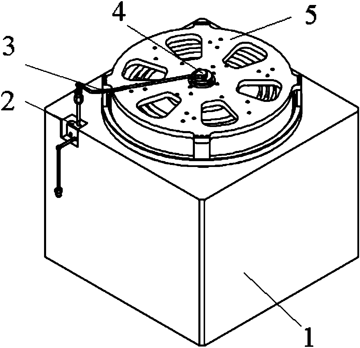
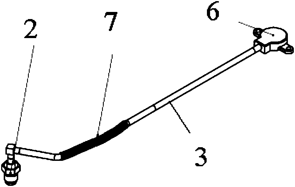
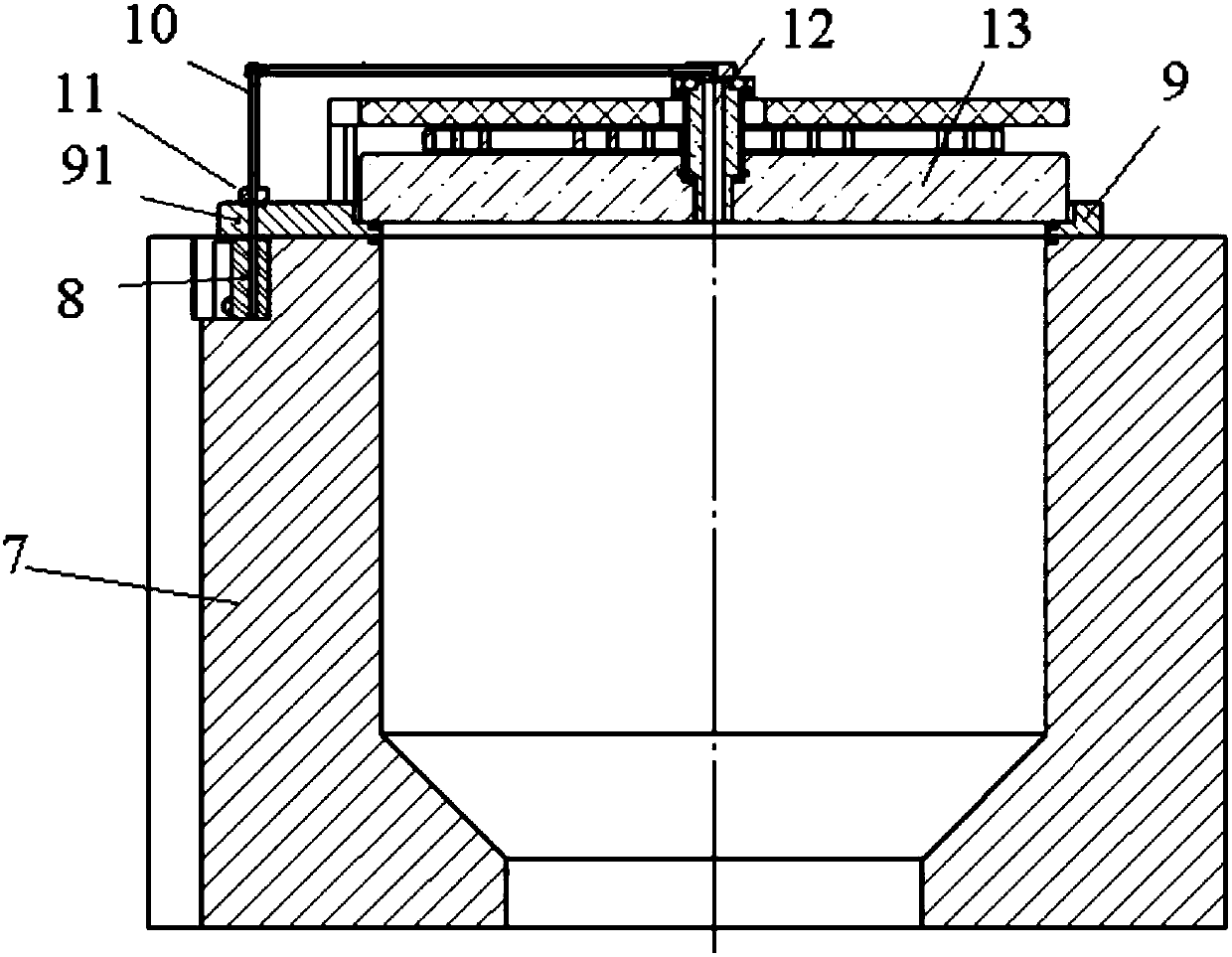
[0033] see image 3 , the reaction chamber provided by the embodiment of the present invention, which includes a cavity 7, a dielectric window 13, a support member 9 for fixing the dielectric window 13 on the top of the cavity 7, and a gas for delivering gas to the inside of the cavity 7 intake mechanism. Wherein, the air intake mechanism includes an air intake channel 91 arranged in the support member 9, and a first pipeline 8 and a second pipeline 10, wherein the first pipeline 8 is arranged on the cavity 7, and is connected with the air inlet One end of the channel 91 is detachably sealed and connected, and the first pipeline 8 is used to deliver gas to the second pipeline 10 through th...


PUM


Abstract

The present invention provides a reaction chamber and a semiconductor processing apparatus. The reaction chamber comprises a cavity, a dielectric window, a support member used for fixing the dielectric window to the top of the cavity, and an air intake mechanism used for conveying gas to the interior of the cavity. The air intake mechanism includes an intake passage disposed in the support member;the air intake mechanism further includes a first pipeline and a second pipeline, the first pipeline is disposed on the cavity and is in detachable seal connection with one end of the intake passage,the first pipeline is configured to transmit gases to the second pipeline through the intake passage; the second pipeline is arranged on the support member and is in fixed seal connection with the other end of the intake passage, and the second pipeline is configured to transmit the gases into the cavity. The reaction cavity simplifies the cavity maintenance process, reduces the maintenance cost,reduces the deposition of reaction by-products in the intake passage and reduces metal pollution, thereby ensuring process results and product yield.

Description

technical field [0001] The invention relates to the technical field of semiconductor manufacturing, in particular to a reaction chamber and semiconductor processing equipment. Background technique [0002] Plasma processing equipment is widely used in processes such as physical vapor deposition, plasma etching and plasma chemical vapor deposition. In order to ensure product yield, strict particle control is generally carried out on the equipment environment, and different processes of plasma etching machines also have special restrictions on metal elements in the process environment. [0003] figure 1 For a block diagram of an existing reaction chamber, see figure 1 , the reaction chamber includes a chamber body 1 and an air inlet mechanism, wherein an upper electrode mechanism 5 including a dielectric window, a coil box, etc. is arranged on the top of the chamber body 1; the air inlet mechanism includes a first pipeline 2, a second pipe Road 3 and intake nozzle 4. Among...

Claims


Application Information

Patent Timeline
Patent Type & Authority Applications(China)
IPC IPC(8): H01J37/32
CPCH01J37/3244H01J37/32458H01J37/32513
Inventor 王伟李一成
Owner BEIJING NAURA MICROELECTRONICS EQUIP CO LTD
Why Eureka
Try Eureka