
A manufacturing method of an OLED touch display module

A technology of touch display and production method, which is applied in the production field of OLED touch display modules, can solve the problems of increasing the weight and thickness of electronic products, failing to meet design requirements, and low production efficiency, so as to ensure that it is not easy to break and the product is guaranteed Quality and yield rate, and the effect of improving production efficiency

Inactive Publication Date: 2019-04-30
TRULY OPTO ELECTRONICS
View PDF6 Cites 0 Cited by
  • Summary
  • Abstract
  • Description
  • Claims
  • Application Information

AI Technical Summary

Problems solved by technology

However, this increases the weight and thickness of electronic products, which cannot meet the increasingly thinner and thinner electronic product design requirements.
Now there is also a technical solution of ON CELL, that is, a solution of directly coating the touch layer on the packaging cover or substrate of the OLED display panel, but the existing ON CELL process is complicated and the production efficiency is low.

Method used


Image

  • A manufacturing method of an OLED touch display module

Examples


Embodiment 1

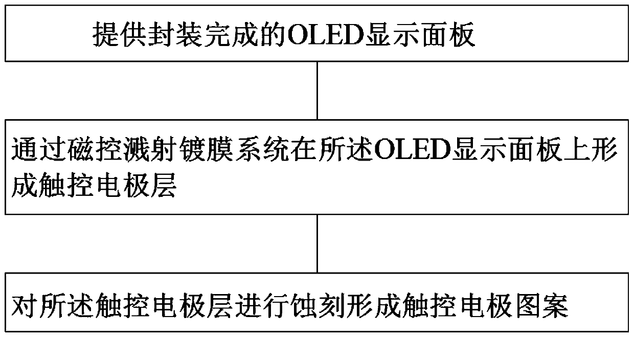
[0029] Such as figure 1 As shown, it represents a manufacturing method of an OLED touch display module provided by the present invention, including the following steps: Step 1: Provide a packaged OLED display panel; Step 2: Apply a magnetron sputtering coating system to the A touch electrode layer is formed on the OLED display panel; step 3: etching the touch electrode layer to form a touch electrode pattern.

[0030] In this way, since the OLED display panel is packaged first, and then the touch electrode layer is directly plated on the packaged OLED display panel, the process can be effectively simplified and the production efficiency can be improved. Compared with the existing method of manufacturing the touch electrode pattern on the substrate and then turning it over to make the OLED functional layer, it can effectively avoid the need to perform complex acid resistance, alkali resistance and resistance to the already formed touch electrode pattern when manufacturing the O...

Embodiment 2

[0039] The principle of this embodiment is the same as that of the previous embodiment, and the steps are similar. The only difference is that in this embodiment, the OLED display panel includes a plurality of sub-display panels; After the touch electrode pattern is completed, the OLED display panel is cut to form multiple OLED touch display module semi-finished products; Step 5: Remove the photoresist covering the touch electrode pattern on each OLED touch display module semi-finished product to form OLED touch display module.

[0040] In this way, the packaged OLED display panel provided in this embodiment is a large board, so that the touch electrode pattern is formed on the large board at the same time and then cut to realize the production of multiple OLED touch display modules at the same time, effectively Increase productivity. Moreover, in this embodiment, after the touch electrode pattern is formed by etching in step 3, the photoresist covering the touch electrode pa...


PUM


Abstract

The invention provides a manufacturing method of an OLED touch display module. The manufacturing method comprises the following steps that 1, providing a packaged OLED display panel; step 2, forming atouch electrode layer on the OLED display panel through a magnetron sputtering coating system; and step 3, etching the touch electrode layer to form a touch electrode pattern. According to the manufacturing method of the OLED touch display module provided by the invention, the touch electrode layer is plated on the packaged OLED display panel and is etched to form the touch electrode pattern; complex protection such as acid resistance, alkali resistance and scratch resistance can be effectively prevented from being carried out on the formed touch electrode pattern when the OLED functional layer is manufactured, so that the process steps and difficulty are effectively simplified, and the production efficiency is improved.

Description

technical field [0001] The invention relates to the field of display technology, in particular to a method for manufacturing an OLED touch display module. Background technique [0002] OLED display technology has been widely used due to its advantages of all-solid-state active light emission, good temperature characteristics, low power consumption, fast response, bendable and foldable, and ultra-thin. When the existing OLED touch display modules integrate touch functions, most of them adopt the method of attaching another layer of touch screen sensors between the OLED display panel and the cover plate. However, this increases the weight and thickness of the electronic product, which cannot meet the increasingly light and thin electronic product design requirements. Now there is also a technical solution of ON CELL, that is, a solution of directly coating the touch layer on the package cover or substrate of the OLED display panel, but the existing ON CELL process is complica...

Claims


Application Information

Patent Timeline
Patent Type & Authority Applications(China)
IPC IPC(8): G06F3/041H01L27/32
CPCG06F3/0412G06F2203/04103H10K59/40
Inventor 李志成
Owner TRULY OPTO ELECTRONICS
Learn More