TVS device chip and manufacturing method thereof

A device chip and device technology, applied in the field of TVS device chips and their manufacturing, can solve problems such as damage, breakdown and loss of electronic components

Pending Publication Date: 2019-04-30
SHANGHAI LEIDITECH ELECTRONICS TECH
View PDF0 Cites 4 Cited by
  • Summary
  • Abstract
  • Description
  • Claims
  • Application Information

AI Technical Summary

Problems solved by technology

[0002] Transient suppression diode TVS products are widely used in applications such as solar inverters, set-top boxes, MOSFET protection, industrial control, telecommunication base stations and power over Ethernet. In practical applications, when the pulse energy exceeds the TVS tube can withstand When the energy is high, the TVS tube will produce overelectric stress damage, which will cause the TVS tube to fail
The most common failure mode of TVS tube is short-circuit failure. At this time, even if the pulse circuit decays, the TVS tube will not return to the initial state, but will always be in the short-circuit state, thereby changing the original circuit structure and causing the electronic equipment to fail. , it may also cause damage to other electronic components due to changes in current or voltage, which violates the original intention of using TVS tubes
If the TVS tube bursts due to excessive short-circuit current and high temperature, it is an open circuit failure at this time, and the impact of the burst itself on electronic equipment and electronic components will be more serious, and even cause other unpredictable losses
Moreover, TVS is widely used in the existing market, but there are often insufficient designs, breakdown, short circuit, affecting the entire circuit board, causing sparks or fires, etc.

Method used


Image

  • TVS device chip and manufacturing method thereof

Examples


Embodiment Construction

[0023] The following will clearly and completely describe the technical solutions in the embodiments of the present invention with reference to the accompanying drawings in the embodiments of the present invention. Obviously, the described embodiments are only some, not all, embodiments of the present invention. Based on the embodiments of the present invention, all other embodiments obtained by persons of ordinary skill in the art without making creative efforts belong to the protection scope of the present invention.

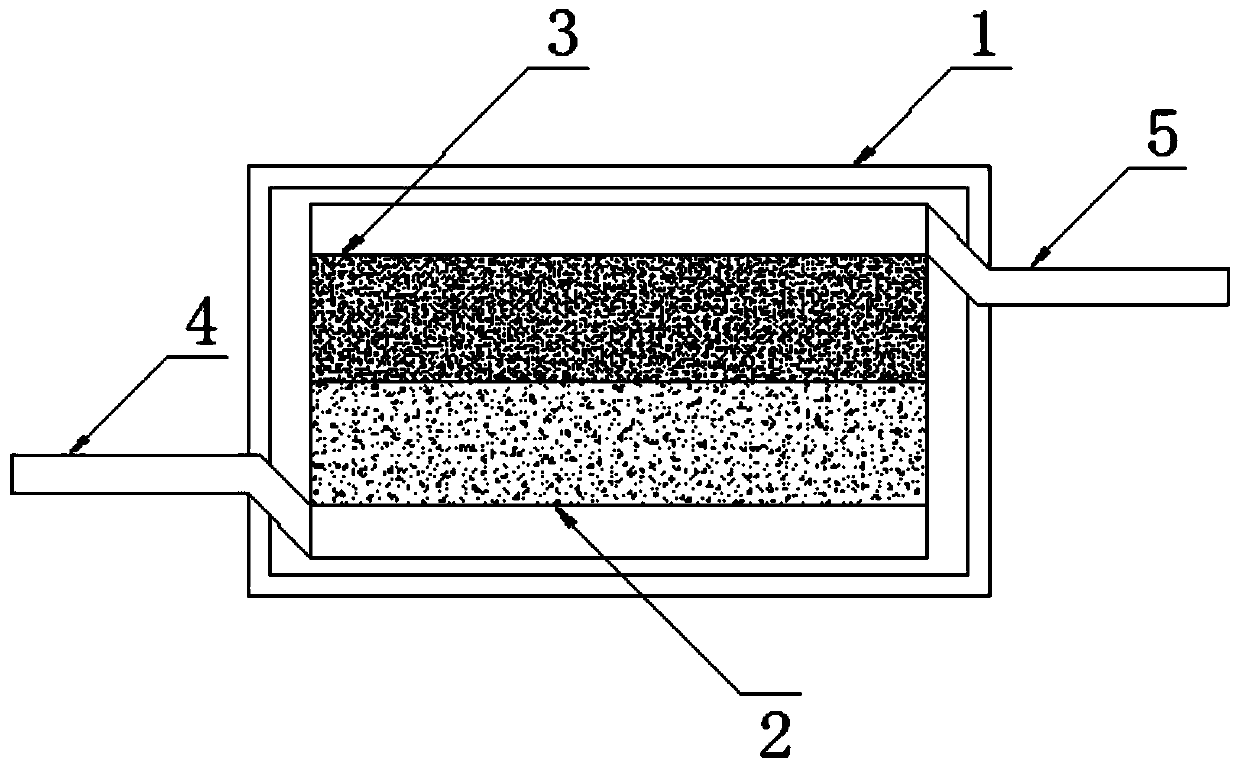
[0024] see figure 1 , the present invention provides a technical solution: a TVS device chip, including a packaging shell 1, a TVS chip layer 2, an overcurrent chip layer 3, a first pin 4 and a second pin 5, and the inner cavity of the packaging shell 1 is set The TVS chip layer 2 and the overcurrent chip layer 3, the bottom of the TVS chip layer 2 is connected to one end of the first pin 4 by wiring, and the other end of the first pin 4 extends to the outside...


PUM


Abstract

The invention discloses a TVS device chip in the technical field of TVS devices. The TVS device chip comprises a package casing, a TVS chip layer, an overcurrent chip layer, a first pin and a second pin. The inner cavity of the package casing is provided with the TVS chip layer and the overcurrent chip layer, the bottom of the TVS chip layer is connected to one end of the first pin by a wire, andthe top of the overcurrent chip layer is connected to one end of the second pin through a wire. Through the novel design of two chips in a TVS, one chip can satisfy a transient voltage clamp protection function, the other chip is automatically disconnected when over-current is continuous, through a high-molecular polymer in a reset over-current filler, when power-off and fault are removed, the collection temperature is reduced, the density of states is increased, the phase transition recovers, nanocrystals are reduced to a chain-like conductive path, the TVS device is restored to a normal state, therefore, the circuit is not short-circuited, and the fire of a circuit is not caused.

Description

technical field [0001] The invention relates to the technical field of TVS devices, in particular to a TVS device chip and a manufacturing method thereof. Background technique [0002] Transient suppression diode TVS products are widely used in applications such as solar inverters, set-top boxes, MOSFET protection, industrial control, telecommunication base stations and power over Ethernet. In practical applications, when the pulse energy exceeds the TVS tube can withstand When the energy is high, the TVS tube will produce overelectric stress damage, which will cause the TVS tube to fail. The most common failure mode of TVS tube is short-circuit failure. At this time, even if the pulse circuit decays, the TVS tube will not return to the initial state, but will always be in the short-circuit state, thereby changing the original circuit structure and causing the electronic equipment to fail. , It may also cause damage to other electronic components due to changes in current o...

Claims


Application Information

Patent Timeline
Patent Type & Authority Applications(China)
IPC IPC(8): H01L23/31H01L25/07H01L21/56H01L29/861
CPCH01L21/561H01L23/3121H01L25/071H01L29/861
Inventor 胡光亮黄志诚
Owner SHANGHAI LEIDITECH ELECTRONICS TECH
Why Eureka
Try Eureka