Method for improving strength of welding pad

A pad and strength technology, applied in the field of printed circuit board design, can solve the problems of reduced soldering area, reduced welding strength, poor welding, etc., and achieve the effect of reasonable layout space and improved strength

Active Publication Date: 2019-05-03
SHANGHAI MITSUBISHI ELEVATOR CO LTD
View PDF3 Cites 2 Cited by
  • Summary
  • Abstract
  • Description
  • Claims
  • Application Information

AI Technical Summary

Problems solved by technology

However, if the dimensions of pad 11 are kept with figure 1 The size of the pad 11 is the same. Since the solder resist window 10 is smaller than the size of the pad, the welding area of ​​the solder must be reduced, which will easily lead to poor soldering or a decrease in welding strength due to insufficient solder volume; if the pad 11 is enlarged The size, to ensure the area and amount of solder required for soldering, will reduce the electrical gap and creepage distance between adjacent pads in the device pad group

Method used


Image

  • Method for improving strength of welding pad
  • Method for improving strength of welding pad
  • Method for improving strength of welding pad

Examples


Embodiment Construction

[0036] The following will clearly and completely describe the technical solutions in the embodiments of the present invention with reference to the accompanying drawings in the embodiments of the present invention. Obviously, the described embodiments are only some of the embodiments of the present invention, not all of them. Based on the embodiments of the present invention, all other embodiments obtained by persons of ordinary skill in the art without creative efforts fall within the protection scope of the present invention.

[0037] It should be noted that, in the case of no conflict, the embodiments of the present invention and the features in the embodiments can be combined with each other.

[0038] The present invention will be further described below in conjunction with the accompanying drawings and specific embodiments, but not as a limitation of the present invention.

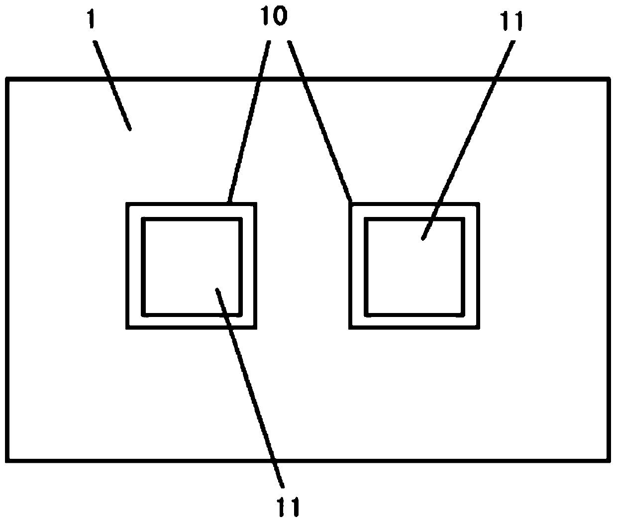
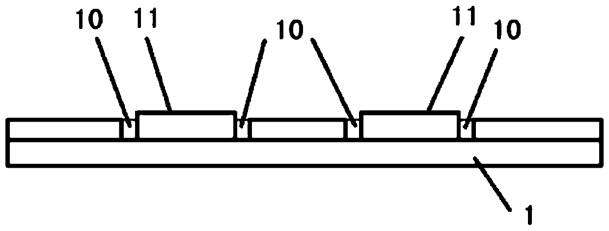
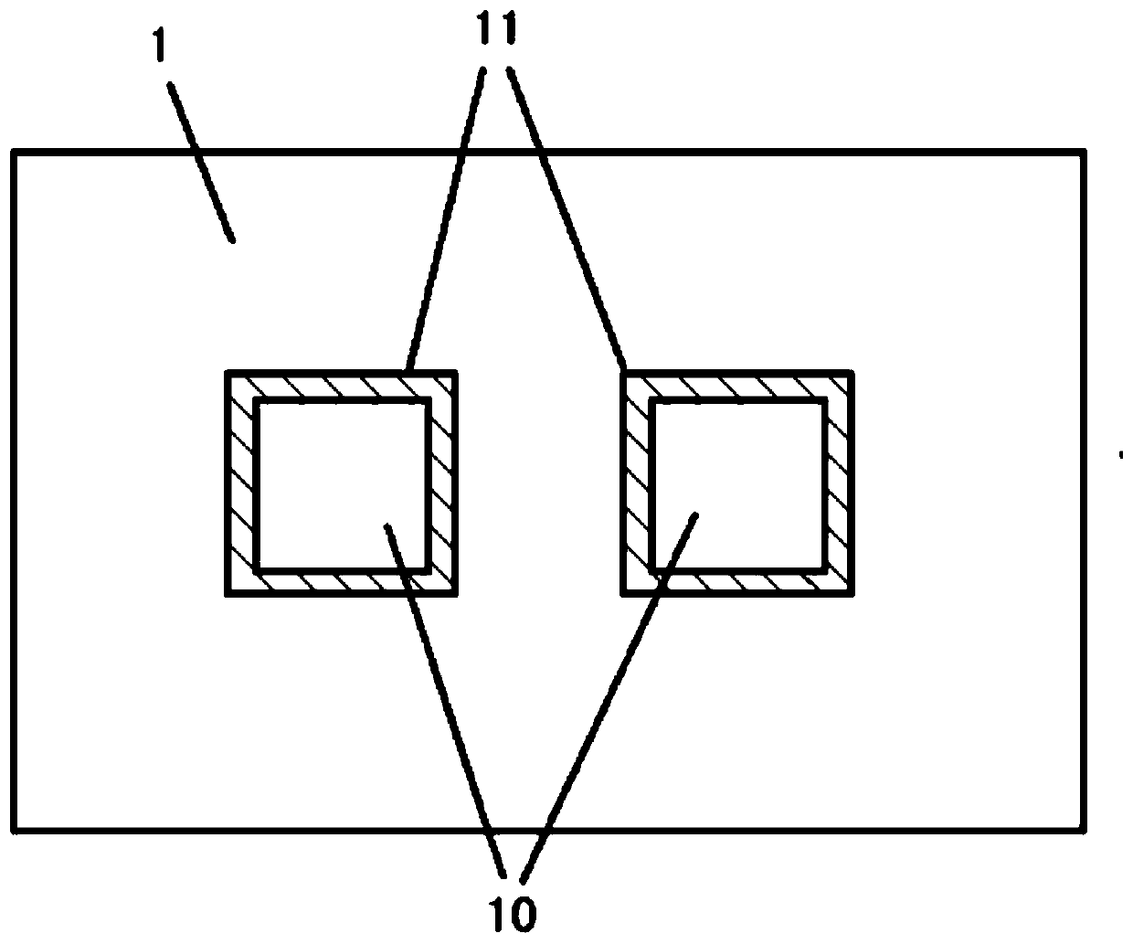
[0039] The present invention includes a method of increasing pad strength such as Figure 6 shown...


PUM


Abstract

The invention discloses a method for improving strength of a welding pad. The method comprises the steps of: acquiring a direction of an external force applied to the welding pad through analysis in advance; determining an expanding direction of the welding pad according to the direction of the external force, expanding the welding pad along the expanding direction, and shrinking a window of a solder mask in the corresponding direction; and covering the edge of the welding pad in the expanding direction with the solder mask. The method has the beneficial effects that: the size of the welding pad and the window of the solder mask are adjusted through analyzing the direction of the external force applied to the welding pad, so that the welding pad is expanded in the expanding direction, thewindow of the solder mask is shrunk along the direction of the external force, thus the solder mask covers the edge of the welding pad in the direction that the external force is applied, the strengthof the welding pad is further improved, the method can neither shrink the electrical spacing of welding pads on a PCB nor affect the welding strength, and the reasonable layout space of the PCB is ensured.

Description

technical field [0001] The invention relates to the technical field of printed circuit board design, in particular to a method for improving the strength of pads. Background technique [0002] With the development of electronic product technology, electronic products are developing in the direction of miniaturization and refinement. The components used in PCB (Printed circuit board, Chinese name: printed circuit board), the pad size of PCB board and the The electrical spacing is gradually reduced, and the strength of the pad is gradually weakened. During the assembly and maintenance of the PCB board, the pads are easy to fall off. Once the pads fall off, it means that the entire PCB board is scrapped. Due to the high cost of the PCB board, the scrapping of the PCB board will bring greater losses to manufacturers and users. . [0003] In the prior art, there are two design methods for pads used for soldering components on the PCB, namely: figure 1 The shown NSMD (Non Solde...

Claims


Application Information

Patent Timeline
Patent Type & Authority Applications(China)
IPC IPC(8): H05K1/18H05K3/22
CPCY02P70/50
Inventor 牛华荣张莉明胡申旦
Owner SHANGHAI MITSUBISHI ELEVATOR CO LTD
Why Eureka
Try Eureka