Two-dimensional layered material-based avalanche field-effect transistor and measurement device

A field-effect transistor, two-dimensional layered technology, applied in the direction of single semiconductor device testing, semiconductor devices, electrical components, etc., can solve the problems of gate voltage losing control of the transistor, unable to completely turn off the transistor, and transistor voltage drop, etc., to achieve small Reset feature, good stability and low energy consumption

Active Publication Date: 2019-05-14
NANJING UNIV
View PDF4 Cites 11 Cited by
  • Summary
  • Abstract
  • Description
  • Claims
  • Application Information

AI Technical Summary

Problems solved by technology

However, silicon-based transistors encounter two fatal bottlenecks in further miniaturization
One is that shrinking device size causes the gate voltage to lose control of the transistor, unable to completely turn off the transistor
Another problem is that the power consumption cannot be reduced, because the thermal emission model limits the subthreshold swing of the field effect transistor at room temperature to less than 60mV / dec
This limits the further reduction of the voltage of the transistor, which limits the realization of low power consumption

Method used


Image

  • Two-dimensional layered material-based avalanche field-effect transistor and measurement device
  • Two-dimensional layered material-based avalanche field-effect transistor and measurement device
  • Two-dimensional layered material-based avalanche field-effect transistor and measurement device

Examples


Embodiment 1

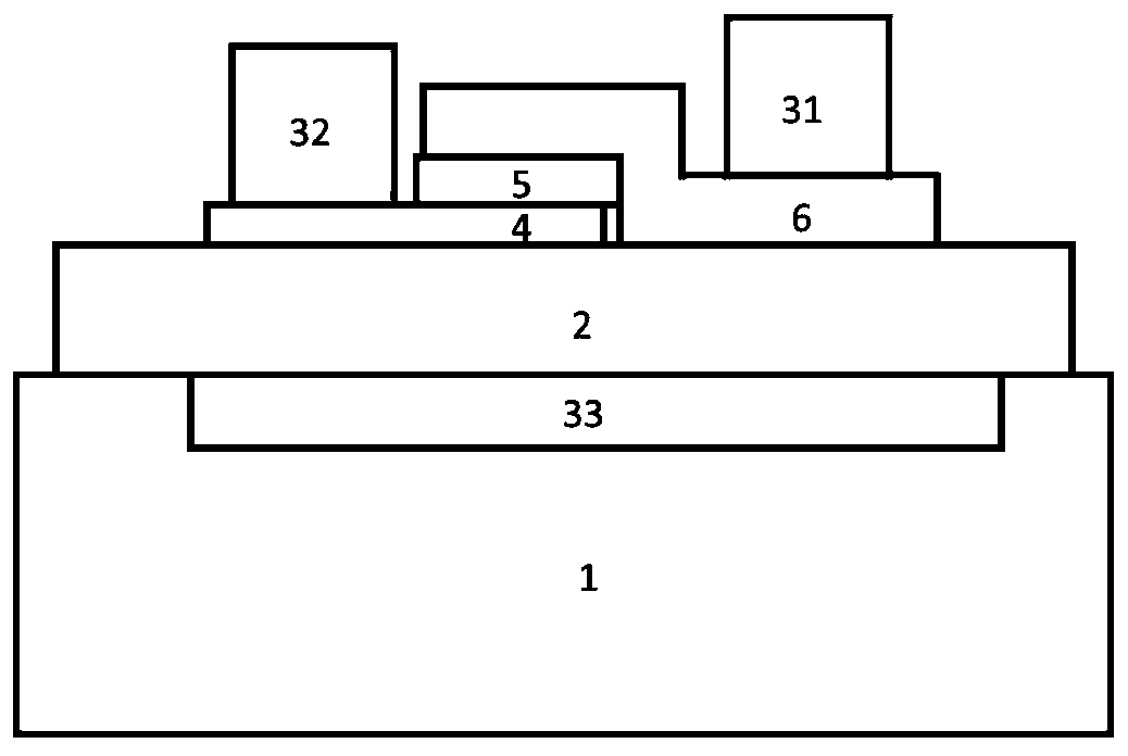
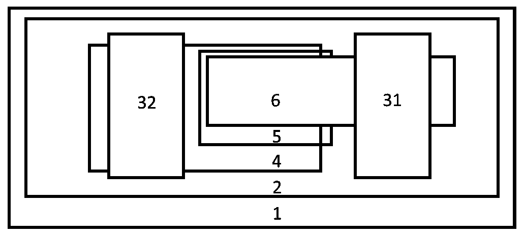
[0025] Such as figure 1 , figure 2 and image 3 As shown, the present embodiment is based on the avalanche field effect transistor of two-dimensional layered materials, including an insulating layer 2, a metal electrode layer, a first two-dimensional material film layer 4, a second two-dimensional material film layer 5 and a third two-dimensional material film layer The thin film layer 6; the metal electrode layer includes a drain electrode layer 31, a source electrode layer 32 and a gate electrode layer 33; the first two-dimensional material thin film layer 4 and the third two-dimensional material thin film layer 6 are laid on the insulating layer 2, the second two The two-dimensional material thin film layer 5 is located between the two stacked parts, the source electrode layer 32 covers the non-stacked part of the first two-dimensional material thin film layer 4, and the drain electrode layer 31 covers the top of the stacked part or the third two-dimensional material thin...

Embodiment 2

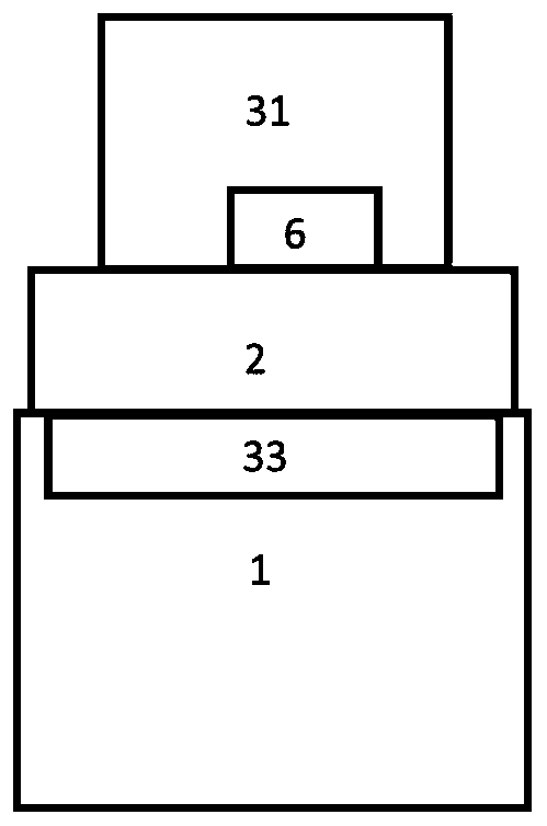
[0049] Such as Figure 6 As shown, the difference between this embodiment and Embodiment 1 is that the gate electrode layer 33 is located above the insulating layer 2, and is connected to the drain electrode layer 31, the source electrode layer 32 and the third two-dimensional material film through another insulating layer 2. Layer 6 connections. The third two-dimensional material thin film layer 5 is an n-type two-dimensional single crystal material, and the second two-dimensional material thin film layer 6 is a p-type two-dimensional single crystal material.

Embodiment 3

[0051] Such as Figure 7 As shown, the difference between this embodiment and Embodiment 1 is that there are two gate electrode layers 33, one is located below the insulating layer 2, and the other is located above the insulating layer 2, and is connected to the drain electrode layer through another insulating layer 2. 31. The source electrode layer 32 is connected to the third two-dimensional material thin film layer 6 .


PUM


Abstract

The invention discloses a two-dimensional layered material-based avalanche field-effect transistor and a measurement device. The transistor comprises an insulation layer, a metal electrode layer, a two-dimensional material thin film layer, a two-dimensional material thin film layer and a two-dimensional material thin film layer, wherein the metal electrode layer comprises a drain electrode layer,a source electrode layer and a gate electrode layer, the two-dimensional material thin film layer and the two-dimensional material thin film layer are laid on the insulation layer, the two-dimensionalmaterial thin film layer is arranged between lamination parts, the source electrode layer covers a non-stack part of the two-dimensional material thin film layer, the drain electrode layer covers a part above the stack parts or the non-stack part of the two-dimensional material thin film layer, and the gate electrode layer is connected with the insulation layer. The measurement device comprises atwo-dimensional layered material-based avalanche field-effect transistor, a voltage source and an ampere meter. By the transistor, the sub-threshold swing of the field-effect transistor is reduced tobe smaller than 1mV/dec, and low power consumption is achieved; and moreover, the device size is reduced, and the device stability is improved.

Description

technical field [0001] The invention relates to a transistor and a measuring device, in particular to an avalanche field effect transistor and a measuring device based on a two-dimensional layered material. Background technique [0002] The rapid development of information technology relies on the continuous increase in the number of transistors and the continuous reduction in transistor size. However, silicon-based transistors have encountered two fatal bottlenecks in further miniaturization. One is that shrinking device dimensions have caused the gate voltage to lose control of the transistor, preventing it from completely turning off the transistor. Another problem is that the power consumption cannot be reduced because the thermal emission model limits the subthreshold swing of the FET to less than 60mV / dec at room temperature. This limits the further reduction of the voltage of the transistor, and also limits the realization of low power consumption. In order to redu...

Claims


Application Information

Patent Timeline
Patent Type & Authority Applications(China)
IPC IPC(8): H01L29/772H01L29/06G01R31/26
Inventor 缪峰王肖沐高安远
Owner NANJING UNIV
Why Eureka
Try Eureka