ESD protection device of SOI power switch

A technology of ESD protection and power switching, which is applied in the direction of semiconductor devices, electric solid state devices, electrical components, etc., and can solve problems affecting protection performance

Active Publication Date: 2019-05-21
INST OF MICROELECTRONICS CHINESE ACAD OF SCI
View PDF7 Cites 3 Cited by
  • Summary
  • Abstract
  • Description
  • Claims
  • Application Information

AI Technical Summary

Problems solved by technology

In some circuits with input ports that need to withstand negative voltage, if the IO voltage is lower than -0.7V and the GND voltage is 0V, when ...

Method used


Image

  • ESD protection device of SOI power switch
  • ESD protection device of SOI power switch

Examples


Embodiment Construction

[0027] Exemplary embodiments of the present disclosure will be described in more detail below with reference to the accompanying drawings. Although exemplary embodiments of the present disclosure are shown in the drawings, it should be understood that the present disclosure may be embodied in various forms and should not be limited by the embodiments set forth herein. Rather, these embodiments are provided for more thorough understanding of the present disclosure and to fully convey the scope of the present disclosure to those skilled in the art.

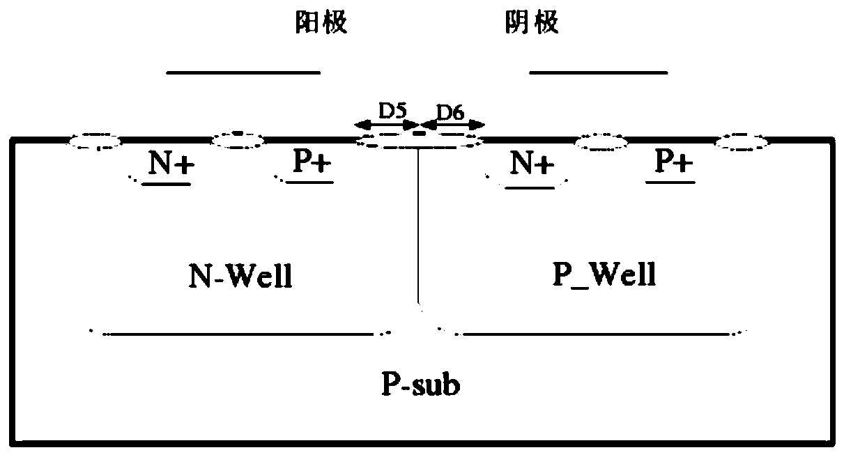
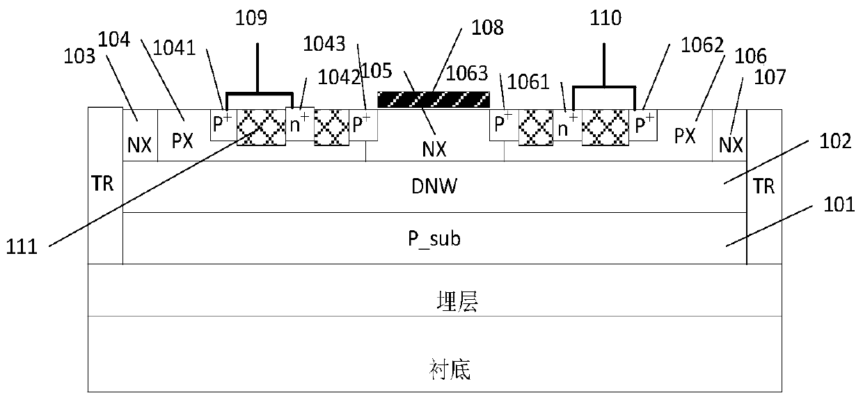
[0028] An embodiment of the present invention provides an ESD protection device for an SOI power switch, such as figure 2 As shown, it includes: a P-type substrate (P_sub) 101; an N-type deep well (DNW) 102 on the P-type substrate 101; a first N well 103, a first P well 104, the second N well 105, the second P well 106, the third N well 107, the width range of the second N well 105 is 2-8 μm; the first P well 104 includes the firs...


PUM

PropertyMeasurementUnit
Lengthaaaaaaaaaa

Abstract

The invention relates to the technical field of semiconductor devices, in particular to an ESD protection device of an SOI power switch. The ESD protection device comprises a P-type substrate, an N-type deep well, a first N well, a first P well, a second N well, a second P well and a third N well, wherein the N-type deep well is arranged on the P-type substrate; the first N well, the first P well,the second N well, the second P well and the third N well are arranged on the N-type deep well in sequence; the width range of the second N well is 2-8 microns; the first P well internally comprisesa first P+ injection area and a first N+ injection area; a second P+ injection area crosses between the first P well and the second N well; the second P well internally comprises a second N+ injectionarea and a fourth P+ injection area; a third P+ injection area crosses between the second N well and the second P well; a gate oxide with a length range of 0.25-6 microns is arranged o the second N well; the first P+ injection area and the first N+ injection area are connected to an anode; and the second N+ injection area and the fourth P+ injection area are connected with a cathode. The ESD protection device is capable of improving the maintaining voltage of the device, reducing the triggering voltage of the device and improving the protection performance.

Description

technical field [0001] The invention relates to the technical field of semiconductor devices, in particular to an ESD protection device for SOI power switches. Background technique [0002] Electrostatic discharge (ESD, Electron Static Discharge) is an instantaneous process in which a large amount of static charge is poured into the integrated circuit from the outside to the inside when the pins of an integrated circuit are floating, and the whole process takes about 1000ns. When the electrostatic discharge of the integrated circuit will generate hundreds or even thousands of volts of high voltage, the gate oxide layer of the input stage in the integrated circuit will be broken down. With the advancement of integrated circuit technology, the feature size of MOS transistors is getting smaller and smaller, and the thickness of the gate oxide layer is getting thinner. In this trend, high-performance ESD protection devices are used to discharge electrostatic charges to protect t...

Claims


Application Information

Patent Timeline
IPC IPC(8): H01L27/02
Inventor 蔡小五曾传滨赵海涛刘海南卜建辉罗家俊
Owner INST OF MICROELECTRONICS CHINESE ACAD OF SCI
Why Eureka
Try Eureka