Display device, display backboard and production method

A display backplane and manufacturing method technology, applied in the direction of electrical components, electrical solid devices, circuits, etc., can solve the problems of high repair time and cost, Micro-LED pixels can not be lit, etc., to achieve high binding efficiency, The effect of high binding yield and simple process

Active Publication Date: 2019-05-21
BOE TECH GRP CO LTD
View PDF6 Cites 25 Cited by
  • Summary
  • Abstract
  • Description
  • Claims
  • Application Information

AI Technical Summary

Problems solved by technology

This method often uses silver paste or solder paste to bind the Micro-LED to the backplane electrode (Pad) (a three-layer structure of ITO-Ag-ITO), but in the process of bonding, a bonding disconnection will occur and cause Micro-LED pixels can't light up
Taking a standard 4K ultra-high definition (Ultra-High Definition, UHD) display screen as an example, a total of 3840×2160=8,294,400 pixels, for RGB Micro-LEDs, a total of 8,294,400×3=24,883,200 Micro-LED chips are required (the number of chips is Tens of millions), but repairing a large number of Micro-LED chips that have failed due to bonding is a difficult problem, and the time and cost of repairing one by one are very high. If Micro-LED bonding with high yield can be carried out on a large area, it will effectively reduce Micro-LED chips. LED Display Backplane Cost

Method used


Image

  • Display device, display backboard and production method
  • Display device, display backboard and production method
  • Display device, display backboard and production method

Examples


Embodiment Construction

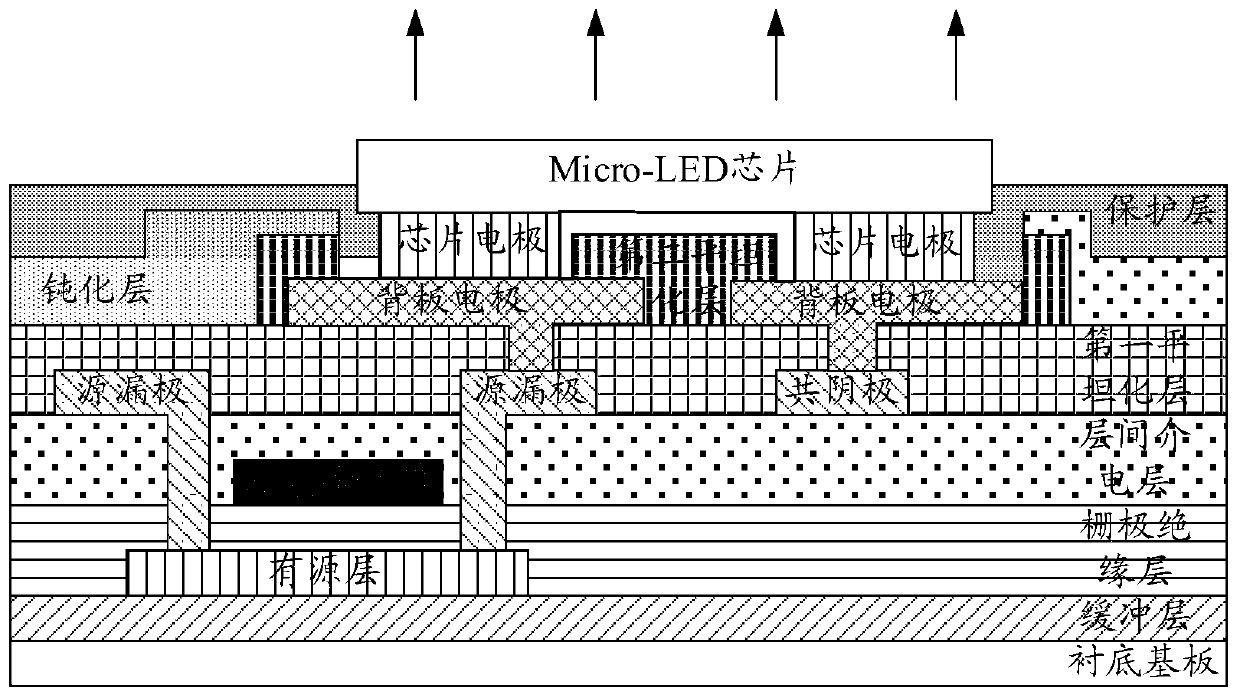
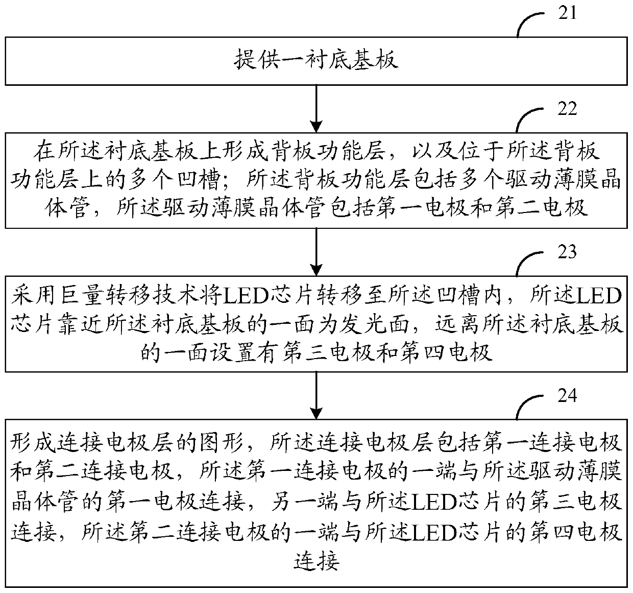
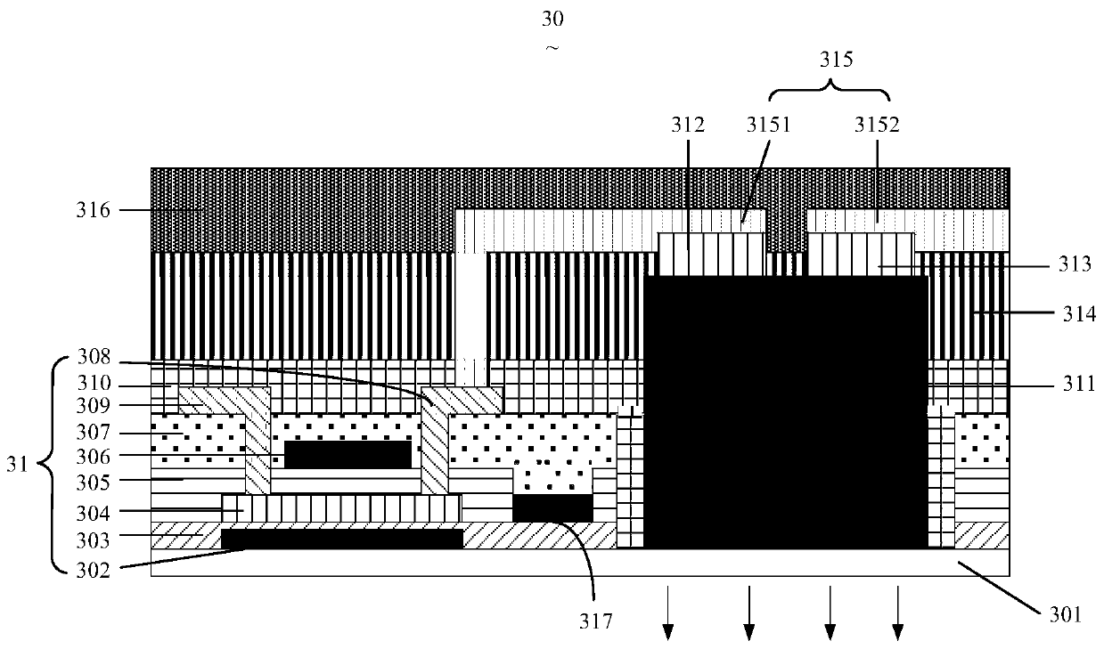
[0036] In order to make the purpose, technical solutions and advantages of the embodiments of the present invention more clear, the following will clearly and completely describe the technical solutions of the embodiments of the present invention in conjunction with the drawings of the embodiments of the present invention. Apparently, the described embodiments are some, not all, embodiments of the present invention. All other embodiments obtained by those skilled in the art based on the described embodiments of the present invention belong to the protection scope of the present invention.

[0037] Unless otherwise defined, the technical terms or scientific terms used in the present invention shall have the usual meanings understood by those skilled in the art to which the present invention belongs. "First", "second" and similar words used in the present invention do not indicate any order, quantity or importance, but are only used to distinguish different components. Words su...


PUM


Abstract

The invention provides a display device, a display backboard and a production method and relates to the technical field of display. The production method comprises the steps of providing a substrate base plate; forming a backboard function layer on the substrate base plate, and forming a plurality of grooves located on the backboard function layer, wherein the backboard function layer comprises aplurality of drive thin film transistors, and the drive thin film transistors comprise first electrodes and second electrodes; transferring LED chips to the grooves through adoption of a mass transfertechnology, wherein faces of the LED chips close to the substrate base plate are light emitting faces, and third electrodes and fourth electrodes are set on the faces of the LED chips away from the substrate base plate; and forming a graph of a connection electrode layer, wherein the connection electrode layer comprises first connection electrodes and second connection electrodes, one end of thefirst connection electrodes is connected with the first electrodes of the drive thin film transistors, the other end is connected with the third electrodes of the LED chips, and one end of the secondconnection electrodes is connected with the fourth electrodes of the LED chips. Binding efficiency and binding yield of the LED chips can be improved, and production cost is reduced.

Description

technical field [0001] The invention relates to the field of display technology, in particular to a display device, a display backplane and a manufacturing method. Background technique [0002] With the development of science and technology, new light emitting diode (Light Emitting Diode, LED) technology is becoming more and more mature. For example: micro light-emitting diode (Micro-LED) technology is to shrink the size of the existing LED to less than 100 microns, which is about 1% of the size of ordinary LEDs. It can transfer micron-level RGB three-color Micro -The LEDs are transferred to the driver substrate to form Micro-LED displays of various sizes. To put it simply, Micro-LED is the thinning, miniaturization and arraying of LEDs. Each Micro-LED pixel can be addressed and driven to emit light independently, and the distance between adjacent pixels is reduced from millimeters to microns. Micro-LED has many advantages such as self-illumination, high brightness, high c...

Claims


Application Information

Patent Timeline
Patent Type & Authority Applications(China)
IPC IPC(8): H01L27/15H01L33/00H01L33/62
Inventor 梁志伟刘英伟吕志军王慧娟王珂曹占锋罗雯倩
Owner BOE TECH GRP CO LTD
Why Eureka
Try Eureka