Semiconductor device

A technology of semiconductors and conductors, applied in the field of semiconductor devices, can solve the problem of increasing the number of parts of 3-phase AC-DC conversion devices, etc.

Pending Publication Date: 2019-05-21
DENSO CORP
View PDF6 Cites 0 Cited by
  • Summary
  • Abstract
  • Description
  • Claims
  • Application Information

AI Technical Summary

Problems solved by technology

Therefore, in addition to multiple chips and current detectors, it is necessary to provide wiring for connecting the chips, which may increase the number of parts of the 3-phase AC-DC converter.

Method used


Image

  • Semiconductor device
  • Semiconductor device
  • Semiconductor device

Examples


no. 1 Embodiment approach

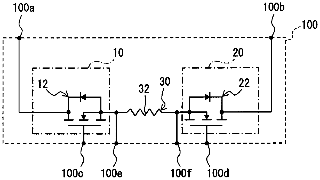
[0020] First, based on figure 1 , the circuit configuration of the semiconductor device 100 will be described.

[0021] The semiconductor device 100 is connected to a current path through which current flows bidirectionally, and forms a part of the current path. The semiconductor device 100 is applicable to, for example, a power supply system including a lithium battery and a lead battery, and a system including an ISG and a lithium battery. In addition, ISG is the abbreviation of Integrated Starter Generator (starter generator).

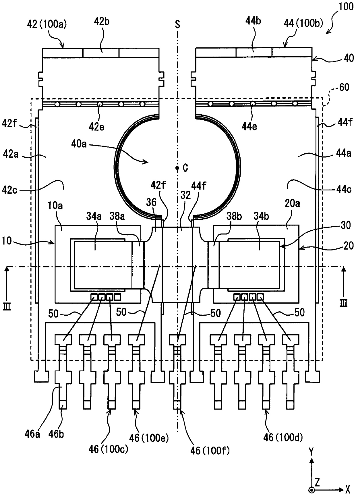
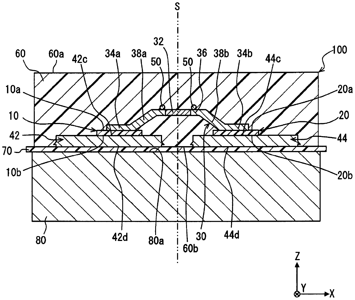
[0022] The semiconductor device 100 includes a first chip 10 , a second chip 20 , and a shunt resistor 30 . The semiconductor device 100 may also be called a semiconductor module. Furthermore, the semiconductor device 100 has, as terminals, a first terminal 100a, a second terminal 100b, control terminals 100c and 100d, and sensing terminals 100e and 100f.

[0023] The first chip 10 has a first switching element 12 . In addition, the second chip...


PUM


Abstract

A semiconductor device is provided with: a first chip (10) including a first switching element (12) that limits a flow of electric current in one direction in a current path; a second chip (20) including a second switching element (22) that limits a flow of electric current in the opposite direction to the one direction in the current path; wiring (30) serving as a relay between the first chip andthe second chip and thereby forming a part of the current path; a lead frame (40) which comprises a first lead (42) with the first chip fixedly arranged thereon and a second lead (44) with the secondchip fixedly arranged thereon, and which forms a current path; and a mold resin (60) which integrally seals the first chip, the second chip, the wiring, and the lead frame. The wiring is a shunt resistance including a resistor (32). The lead frame further includes a sense terminal (100e, 100f, 46) for detecting a voltage drop across the resistor.

Description

[0001] This application claims priority based on Japanese Patent Application No. 2016-199127 filed on October 7, 2016, the content of which is cited here. technical field [0002] The present invention relates to a semiconductor device including a plurality of chips including semiconductor elements and wirings connecting the chips. Background technique [0003] Conventionally, as described in Patent Document 1, a three-phase AC-DC conversion device including a bidirectional switch and a current detector is known. A bidirectional switch has a pair of switching elements connected to each other. In the bidirectional switch, the current flowing through the current path is restricted by both switching elements being turned off. In addition, the current detector is connected to one switching element, and detects the current flowing through the bidirectional switch. [0004] prior art literature [0005] patent documents [0006] Patent Document 1: Japanese Patent Laid-Open No....

Claims


Application Information

Patent Timeline
Patent Type & Authority Applications(China)
IPC IPC(8): H01L25/07H01L23/48H01L25/18
CPCH01L2224/40137H01L25/18H01L2924/18301H01L23/49524H01L23/49562H01L2224/48247H01L23/4006H01L23/49575H01L2924/13091H01L2924/13055H01L25/072H01L23/3107H01L2924/19107H01L2224/04034H01L2224/04042H01L2224/73221H01L2224/06181H01L24/37H01L2224/291H01L2224/73263H01L2924/1815H01L2224/32245H01L2924/19104H01L2924/19043H01L24/06H01L24/29H01L24/32H01L24/40H01L24/48H01L24/73G01R1/203H01L2224/37111H01L2224/834H01L2224/37155H01L2224/40499H01L2224/45099H01L2224/37149H01L2224/37147H01L2224/05599H01L2224/0603H01L2224/84801H01L24/84H01L2224/49171H01L2924/00014H01L2924/00H01L2924/014H01L2924/013H01L2924/01025H01L2924/01029H01L2924/0105H01L2924/01028H01L23/49541H01L23/3121G01R19/0092G01R15/146H01L2023/4087H01L2023/4031H01L2224/48137H01L2224/45111H01L2224/45147H01L2224/45155H01L2224/45149H01L25/07H01L23/48
Inventor 林敬昌户本俊介森勇辅
Owner DENSO CORP
Why Eureka
Try Eureka