Package substrate, semiconductor device and manufacturing method thereof

A manufacturing method and semiconductor technology, applied in the direction of semiconductor devices, electric solid devices, electrical components, etc., can solve problems such as the inability of the white glue layer to adapt, loss of displacement ability, and cracking, so as to improve adaptability, delay cracking time, and relieve heat. The effect of stress

Pending Publication Date: 2019-05-24
APT ELECTRONICS
View PDF0 Cites 4 Cited by
  • Summary
  • Abstract
  • Description
  • Claims
  • Application Information

AI Technical Summary

Problems solved by technology

However, due to the heat generated by the semiconductor device during use, the white glue layer will generate thermal stress under the action of thermal expansion and contraction, and then produce thermal expansion and cold contraction displacement; at the same time, the white glue layer will lose its The white oil inside will continue to precipitate, and will gradually lose its displacement ability, so the white glue layer is easy to crack because it cannot adapt to the displacement of thermal expansion and contraction

Method used


Image

  • Package substrate, semiconductor device and manufacturing method thereof
  • Package substrate, semiconductor device and manufacturing method thereof
  • Package substrate, semiconductor device and manufacturing method thereof

Examples


Embodiment 1

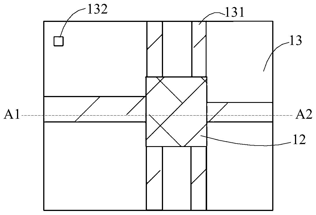
[0040] See figure 1 , is a top view of a semiconductor device according to Embodiment 1 of the present invention.

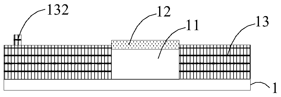
[0041] Such as figure 1 and figure 2 As shown, this semiconductor device includes: a crystal-bonding substrate 1, an LED chip 11 disposed on the crystal-bonding substrate 1, a fluorescent sheet 12 disposed on the LED chip 11, and a fluorescent sheet 12 disposed on the LED chip 11 and the fluorescent sheet 12. White glue layer 13 around; wherein, the top of white glue layer 13 is flush with the upper surface of fluorescent sheet 12, and the upper surface of white glue layer 13 is provided with at least one groove 131, and this at least one groove 131 runs through white glue On the inner wall and the outer wall of the layer 13 , the groove extension direction of at least one groove 131 is perpendicular to the side of the LED chip 11 .

[0042] Compared with the prior art, in the semiconductor device of the present invention, since the upper surface of the white...

Embodiment 2

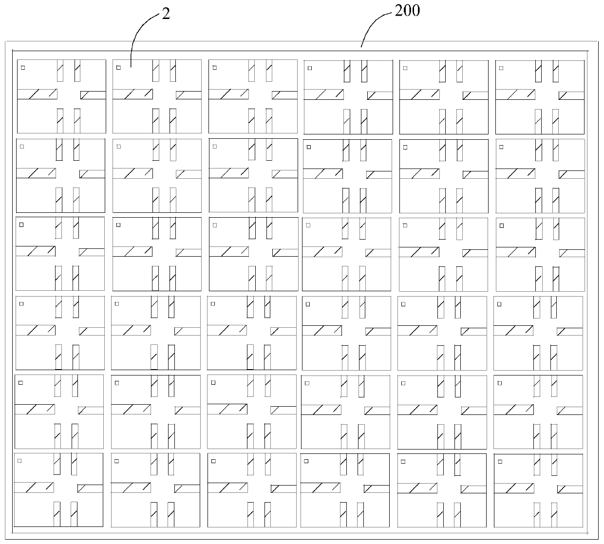
[0048] Such as Figure 3 ~ Figure 5 As shown, the present invention also provides a packaging substrate, which includes: a temporary substrate 200 and a die-bonding substrate 100; wherein, the temporary substrate 100 has a die-bonding area 2, and the die-bonding 2 is arranged at a preset distance and is provided with at least A convex strip 21 and a first through hole 22, one end of at least one convex strip 21 surrounds the fluorescent sheet mounting area 23, and the other end is connected to the edge of the crystal bonding area 2; the crystal bonding substrate 100 is used to fix LEDs at a preset distance Chip 11; when the temporary substrate 200 and the crystal-bonding substrate 100 are aligned and attached, the LED chip 11 fixed on the crystal-bonding substrate 100 is bonded one-to-one with the fluorescent sheet arranged in the fluorescent sheet mounting area 23; After the white glue is injected between the combined temporary substrate 200 and the die-bonding substrate 100,...

Embodiment 3

[0051] The present invention also provides a method for manufacturing a semiconductor device, the following in conjunction with the attached Figure 3 ~ Figure 5 , to describe the preparation method in detail.

[0052] The manufacturing method of the semiconductor device comprises the following steps:

[0053] S1, provide a temporary substrate (such as Figure 6 a); where, if image 3 and Figure 4 As shown, the temporary substrate 200 has a crystal-bonding area 2, the crystal-bonding area 2 is arranged at a preset interval and is provided with at least one convex strip 21 and a first through hole 22, and one end of the at least one convex strip 21 is surrounded by a The fluorescent sheet installation area 23, the other end is connected with the edge of the crystal bonding area 2;

[0054] S2. Use double-sided tape to paste the fluorescent sheet in the fluorescent sheet installation area (such as Figure 6 b);

[0055] Wherein, step S2 includes:

[0056] S21. Provide a ...


PUM


Abstract

The invention discloses a package substrate, a semiconductor device and a manufacturing method thereof. The semiconductor device comprises a die bonding substrate, an LED chip disposed on the die bonding substrate, a fluorescent sheet disposed on the LED chip, and a white glue layer disposed around the LED chip and fluorescent sheet; the top of the white glue layer is flush with the upper surfaceof the fluorescent layer; at least one groove is formed in the upper surface of the white glue layer; the at least one groove passes through the inner wall and outer wall of the white glue layer; andthe groove extension direction of the at least one groove is perpendicular to the side of the LED chip. With the semiconductor device and the manufacturing method thereof of the invention adopted, thethermal stress of the white glue layer can be effectively alleviated, the adaptability of the white glue layer to heat-induced expansion and cold-induced contraction displacement can be improved, andtherefore, the cracking time of the white glue layer can be delayed, and the service life of the semiconductor device can be prolonged.

Description

technical field [0001] The invention relates to the technical field of LEDs, in particular to a packaging substrate, a semiconductor device and a manufacturing method thereof. Background technique [0002] Traditional semiconductor devices usually use silicone resin mixed with phosphor to package LED chips. Due to the poor weather resistance and thermal stability of silicone resin, it brings light decay, light color shift, and yellowing to semiconductor devices. And other issues. [0003] In order to solve the above-mentioned problems of traditional semiconductor devices, existing semiconductor devices are packaged by using fluorescent sheets with good weather resistance and high thermal stability. Among them, during the packaging process of the semiconductor device, a white glue layer is generally arranged around the fluorescent sheet to prevent light leakage and improve the light extraction efficiency of the semiconductor device. However, due to the heat generated by the...

Claims


Application Information

Patent Timeline
Patent Type & Authority Applications(China)
IPC IPC(8): H01L25/075H01L33/48H01L33/50H01L33/54H01L33/64
Inventor 李真真朱文敏万垂铭刘锐吴俊健曾照明肖国伟
Owner APT ELECTRONICS
Why Eureka
Try Eureka