Transient voltage suppression device

A technology for suppressing device and transient voltage, applied in circuits, electrical components, electrical solid devices, etc., can solve the problem of high snapback voltage

Active Publication Date: 2019-05-28
NUVOTON
View PDF3 Cites 0 Cited by
  • Summary
  • Abstract
  • Description
  • Claims
  • Application Information

AI Technical Summary

Problems solved by technology

[0004] However, existing transient voltage suppression devices are not satisfactory in all respects
For example: the second breakdown trigger current (It2) is too low, the snapback voltage (Snack back voltage) is too high, etc.

Method used


Image

  • Transient voltage suppression device
  • Transient voltage suppression device
  • Transient voltage suppression device

Examples


no. 1 example

[0041] The transient voltage suppression device of this embodiment includes a first heavily doped region disposed in a well and a second heavily doped region disposed under the first heavily doped region. The above-mentioned first heavily doped region and the second heavily doped region have opposite conductivity types, so as to reduce the snapback voltage of the transient voltage suppression device.

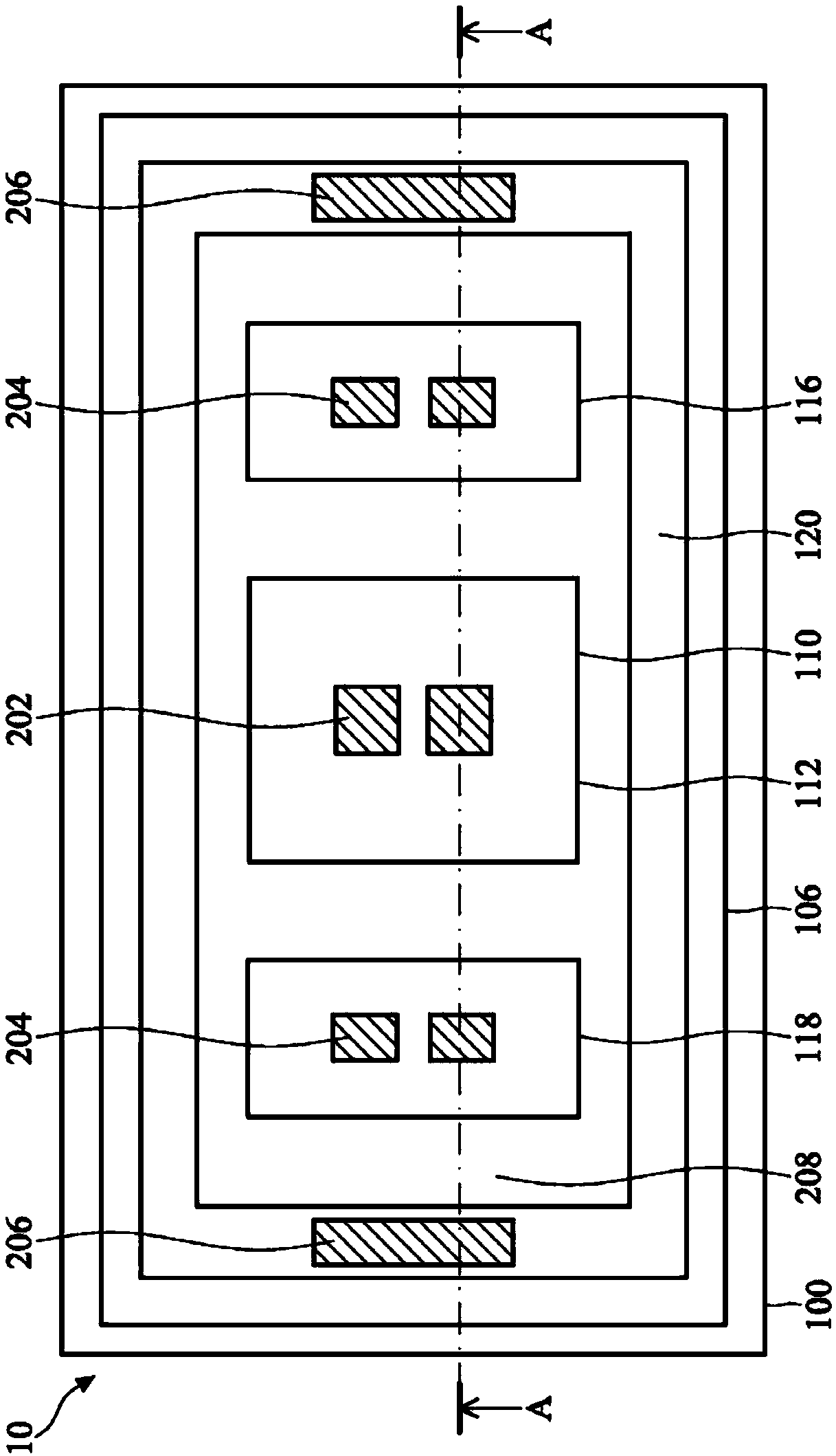
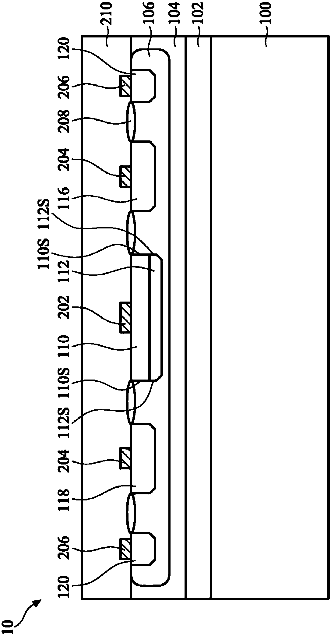
[0042] Figure 1A and Figure 1B A top view and a cross-sectional view of the transient voltage suppression device 10 of this embodiment are shown. In detail, Figure 1B for along Figure 1A The section view obtained by section line A-A.

[0043] Such as Figure 1A and Figure 1B As shown, the transient voltage suppression device 10 of this embodiment generally includes a substrate 100, a first semiconductor layer 102 disposed on the substrate 100, a second semiconductor layer 104 disposed on the first semiconductor layer 102, and a second semiconductor layer 104 disposed on ...

no. 2 example

[0080] One difference between this embodiment and the first embodiment is that the transient voltage suppression device of this embodiment includes a separate second heavily doped region of the first conductivity type disposed under the first heavily doped region of the second conductivity type. region and the third heavily doped region, which can further increase the secondary breakdown current and further reduce the snapback voltage.

[0081] It should be noted that, unless otherwise specified, the same or similar components in this embodiment and the previous embodiments will be denoted by the same reference numerals, and their forming methods can also be the same or similar to those of the previous embodiments.

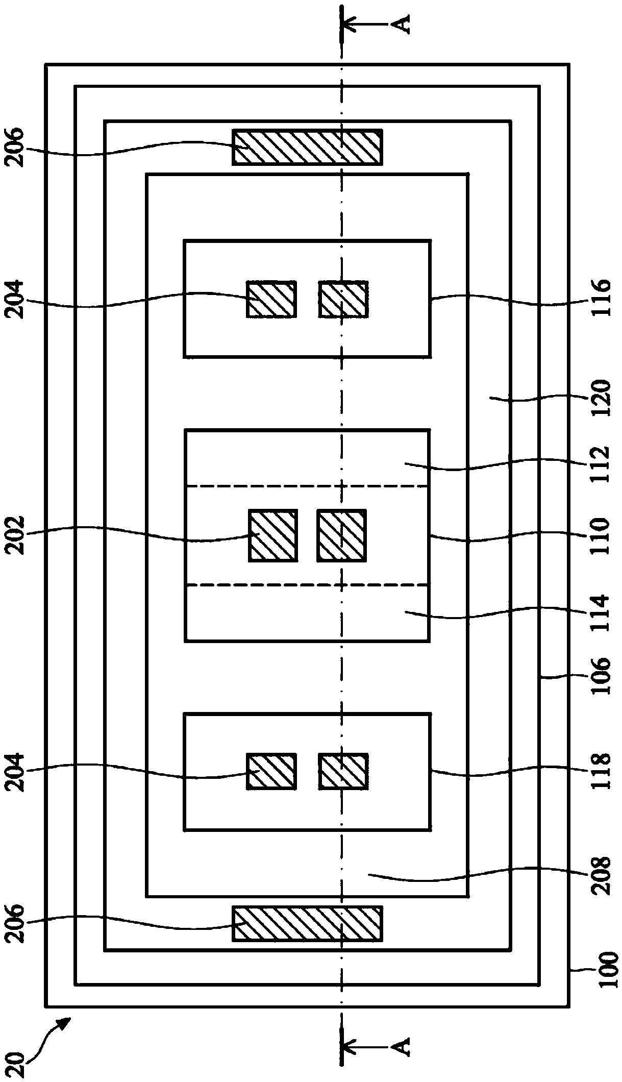
[0082] Figure 2A and Figure 2B A top view and a cross-sectional view of the transient voltage suppression device 20 of this embodiment are shown. In detail, Figure 2B for along Figure 2A The section view obtained by section line A-A.

[0083] Such as Figu...

no. 3 example

[0092] One difference between this embodiment and the second embodiment is that the transient voltage suppression device of this embodiment includes a first well and a second well of the first conductivity type separated, which can further increase the secondary breakdown current and further reduce the snapback Voltage.

[0093] It should be noted that, unless otherwise specified, the same or similar components in this embodiment and the previous embodiments will be denoted by the same reference numerals, and their forming methods can also be the same or similar to those of the previous embodiments.

[0094] Figure 3A and Figure 3B A top view and a cross-sectional view of the transient voltage suppression device 30 of this embodiment are shown. In detail, Figure 3B for along Figure 3A The section view obtained by section line A-A.

[0095] Such as Figure 3A and Figure 3B As shown, the second semiconductor layer 104 of the second conductivity type of the transient ...


PUM


Abstract

Embodiments of the present invention provide a transient voltage suppression device. The transient voltage suppression device includes a substrate, a first semiconductor layer of a first conductivitytype disposed on the substrate, a second semiconductor layer of a second conductivity type disposed on the first semiconductor layer, and a first well and a second well of the first conductivity typedisposed in the second semiconductor layer. The second well is disposed adjacent to the first well but separated from each other. The transient voltage suppression device further includes a first heavily doped region disposed between the first well and the second well and extending into the second conductivity type of the first well and the second well, a second heavily doped region of the first conductivity type disposed in the first well under the first heavily doped region, and a third heavily doped region of the first conductivity type disposed in the second well under the first heavily doped region. The transient voltage suppression device can reduce the snapback voltage of the transient voltage suppression device and further increase the secondary breakdown current.

Description

technical field [0001] The embodiments of the present invention relate to a semiconductor device, and in particular to a transient voltage suppression device. Background technique [0002] Transient voltage suppression devices have been widely used in various electronic products, such as high power devices, personal computers, mobile phones, and digital cameras, for example. [0003] Transient voltage suppressors are generally used to protect integrated circuits from damage caused by accidental transient overvoltage (or current) events such as electrostatic discharge (ESD), fast transient voltage (or current) or lightning. When the instantaneous voltage suppression device is subjected to the above-mentioned instantaneous overvoltage (or current) event, its working impedance can be reduced to an extremely low conduction value, thereby allowing a large current to pass through while clamping the voltage at a predetermined level. Therefore, the transient voltage suppression dev...

Claims


Application Information

Patent Timeline
Patent Type & Authority Applications(China)
IPC IPC(8): H01L27/08H01L29/06H01L21/82
Inventor 阿南德陈柏安
Owner NUVOTON
Why Eureka
Try Eureka