Split-gate SONOS (Semiconductor Oxide Nitride Oxide Semiconductor) memory device

A storage device and split-gate technology, which is applied in the direction of electric solid-state devices, semiconductor devices, electrical components, etc., can solve problems such as affecting, degrading device performance, reducing device channel mobility, etc., to reduce manufacturing costs and improve device performance. Effect

Active Publication Date: 2019-05-28
SHANGHAI HUAHONG GRACE SEMICON MFG CORP
View PDF4 Cites 1 Cited by
  • Summary
  • Abstract
  • Description
  • Claims
  • Application Information

AI Technical Summary

Benefits of technology

The inventive technology allows for better control over how much charge can be stored on certain parts within one chip without compromising its overall functioning well. This results from injecting nitrogen gas (N2) during production processes that create silicon dioxide layers inside the chips's active area called gate oxides. By controllably distributing this dopant throughout these regions, it becomes possible to achieve specific desired properties such as lower leakage current and reduced power consumption compared with traditional methods like adding extra mask steps after fabrication.

Problems solved by technology

This patented technical problem addressed in this patents relates to improving the efficiency and reliability of semiconductoreflectronic memories like FinFETS or MESCIs while reducing their size without sacrificially compromising data retention capabilities.

Method used


Image

  • Split-gate SONOS (Semiconductor Oxide Nitride Oxide Semiconductor) memory device
  • Split-gate SONOS (Semiconductor Oxide Nitride Oxide Semiconductor) memory device
  • Split-gate SONOS (Semiconductor Oxide Nitride Oxide Semiconductor) memory device

Examples


Embodiment 1

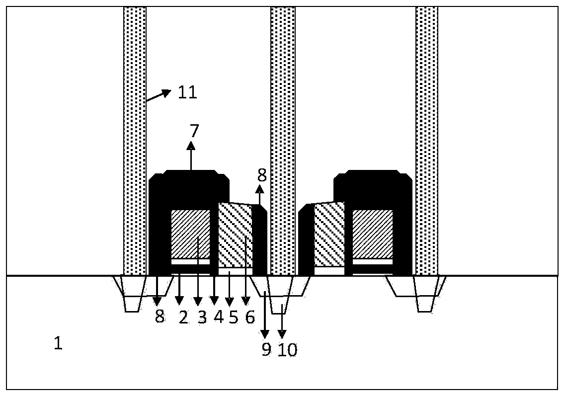
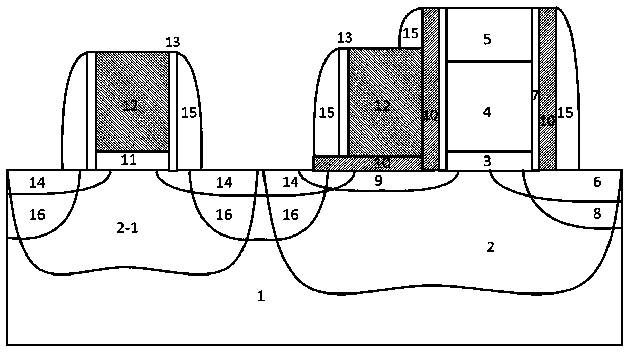
[0023] like figure 2 as shown, figure 2 It is a schematic structural diagram of a split-gate SONOS memory device according to the present invention. In this embodiment, the device structure includes: a P-type substrate 1 and a gate oxide layer 3 and an ONO oxynitride layer 10 formed on the P-type substrate 1; the gate oxide layer 3 is used to form the selection The gate oxide layer of the tube; the oxynitride layer 10 is a multi-layer structure of oxide layer-nitride layer-oxide layer, which is used as the ONO layer of the storage tube; the gate oxide layer 3 is sequentially provided with a polysilicon gate 4 and a selection transistor polysilicon gate The top oxide layer 5 on the polysilicon gate 4 of the selection transistor forms a stacked structure; that is, the three-layer structure located on the upper surface of the substrate from bottom to top is: the gate oxide layer 3, the selection transistor Polysilicon gate 4, top oxide layer 5.

[0024] The split-gate SONOS ...

Embodiment 2

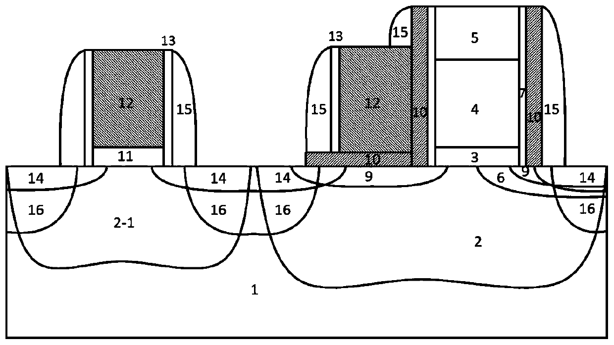
[0034] like image 3 as shown, image 3 It is a schematic structural diagram of another split-gate SONOS storage device of the present invention. In this embodiment, the device structure includes: a P-type substrate 1 and a gate oxide layer 3 and an ONO oxynitride layer 10 formed on the P-type substrate 1; the gate oxide layer 3 is used to form the selection The gate oxide layer of the tube; the oxynitride layer 10 is a multi-layer structure of oxide layer-nitride layer-oxide layer, which is used as the ONO layer of the storage tube; the gate oxide layer 3 is sequentially provided with a polysilicon gate 4 and a selection transistor polysilicon gate The top oxide layer 5 on the polysilicon gate 4 of the selection transistor forms a stacked structure; that is, the three-layer structure located on the upper surface of the substrate from bottom to top is: the gate oxide layer 3, the selection transistor Polysilicon gate 4, top oxide layer 5.

[0035] The split-gate SONOS stora...


PUM


Abstract

The invention provides a split-gate SONOS (Semiconductor Oxide Nitride Oxide Semiconductor) memory device. The split-gate SONOS memory device comprises a gate oxide layer and a nitrogen oxide layer which are formed on a substrate, wherein a selection tube polysilicon gate, a top end oxide layer and an isolation layer are arranged on the gate oxide layer; a memory tube polysilicon gate is arrangedon the nitrogen oxide layer; the nitrogen oxide layer and one side of the memory tube polysilicon gate are close to the isolation layer; a memory tube P-type well is positioned below the selection tube polysilicon gate and the memory tube polysilicon gate; the substrate channel between the source end of the selection tube and the selection tube polysilicon gate is provided with a P-type boron injection region; and the channel of the P-type substrate below the memory tube polysilicon gate is provided with an N-type arsenic injection region. According to the invention, a single-side boron injection region of the selection tube and a source-end single-side arsenic or antimony injection region are formed, and boron in the boron injection region is diffused into a channel of the selection tubeto realize threshold voltage adjustment of the selection tube; an N-type arsenic injection region is formed through the threshold voltage adjustment of the memory tube; and finally, threshold voltageadjustment of the selection tube and threshold voltage adjustment of the memory tube device are not influenced mutually, the device performance is improved, and the manufacturing cost is reduced.

Description


Claims


Application Information

Patent Timeline
Owner SHANGHAI HUAHONG GRACE SEMICON MFG CORP
Why Eureka
Try Eureka