Measuring mechanism and method for dielectric constant of dielectric substrate
A technology of dielectric substrate and permittivity, which is used in the measurement of electrical variables, measurement devices, and resistance/reactance/impedance measurement, etc. The effect of accurate measurement results
- Summary
- Abstract
- Description
- Claims
- Application Information
AI Technical Summary
Problems solved by technology
Method used
Image
Examples
Embodiment 1
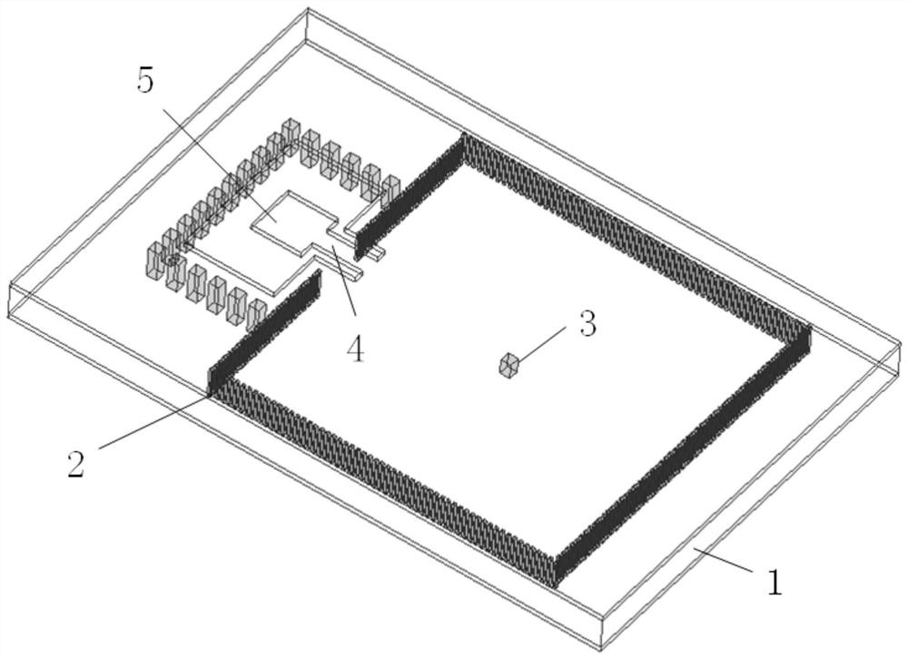
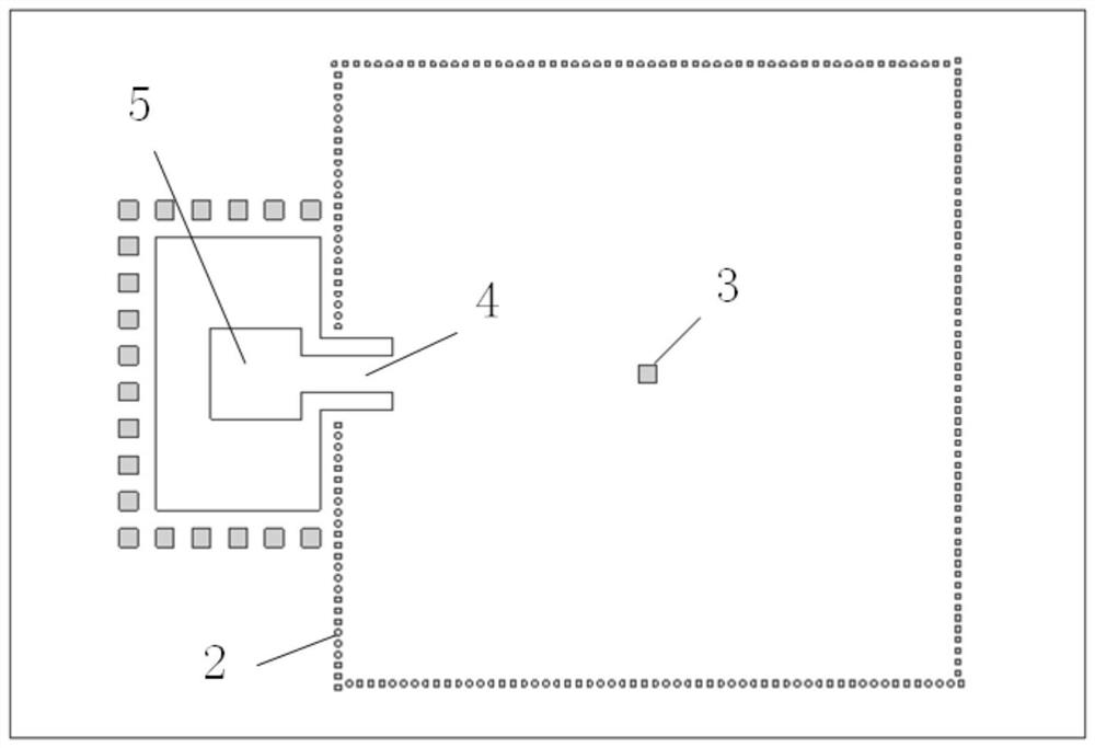
[0043] like figure 1 and figure 2 shown, at a thickness of h sub Three substrate-integrated waveguide resonators 2 are respectively arranged on the dielectric substrate 1 of =6.52um. The cavity sizes of the three substrate-integrated waveguide resonators 2 are all 340um×340um. Metallized blind holes 3 are provided in the middle of the body, which are the first square metallized blind hole 31, the second square metallized blind hole 32, and the first square metallized blind hole 33, so that the dielectric substrate 1 Sample 1, sample 2, and sample 3 are respectively formed on the above. For details, refer to Figure 3 ~ Figure 5 . In this embodiment, the three metallized blind holes 3 are all square structures with the same side length and different heights, and the height of the first square metallized blind hole 31 is h 1 =0um, side length is l 1 =8um; the height of the second square metallized blind hole 32 is h 2 =2.76um, side length is l 1 =8um; the height of the t...
Embodiment 2
[0056] like figure 1 and figure 2 shown, at a thickness of h sub Three substrate-integrated waveguide resonators 2 are respectively arranged on the dielectric substrate 1 of =6.52um. The cavity sizes of the three substrate-integrated waveguide resonators 2 are all 340um×340um. Metallized blind holes 3 are provided in the middle of the body. They are respectively the fourth square metallized blind hole 34, the fifth square metallized blind hole 35, and the sixth square metallized blind hole 36, so that sample 4, sample 5 and sample 6 are respectively formed on the dielectric substrate 1. For details, refer to Figure 6 ~ Figure 8 . In this embodiment, the three metallized blind holes 3 are all square structures with the same height and different side lengths, and the height of the fourth square metallized blind hole 34 is h 4 =5.52um, the side length is l 4 =0um; the height of the fifth square metallized blind hole 35 is h 4 =5.52um, the side length is l 5 =2um; the hei...
Embodiment 3
[0070] In this embodiment, the methods of Embodiment 1 and Embodiment 2 are compared with several traditional dielectric constant measurement methods respectively, and the specific data are shown in the following table:
[0071]
[0072] According to the above table, it can be seen that in the high-frequency band, the de-embedding method of the traditional dielectric constant measurement not only does not help the accuracy improvement but worsens the result. This is because in the millimeter-wave, submillimeter-wave and even terahertz frequency bands, the size of the feed structure is comparable to that of the resonator itself, and the influence of the feed structure on the structure of the resonator cannot be ignored. However, the dielectric constant measurement method shown in the present invention provided by Examples 1 and 2 shows the accuracy that other traditional methods in this frequency band do not have. At the same time, the method is easy to operate, simple in pro...
PUM
 Abstract
Description
Claims
Application Information
 - R&D
- Intellectual Property
- Life Sciences
- Materials
- Tech Scout
- Unparalleled Data Quality
- Higher Quality Content
- 60% Fewer Hallucinations
Browse by: Latest US Patents, China's latest patents, Technical Efficacy Thesaurus, Application Domain, Technology Topic, Popular Technical Reports.
© 2025 PatSnap. All rights reserved.Legal|Privacy policy|Modern Slavery Act Transparency Statement|Sitemap|About US| Contact US: help@patsnap.com


